Power Semiconductor Devices

More on this category »

Latest Post

Showing posts with label Electronic Converter. Show all posts

Implementation of One cycle control technique for Buck converter

PRESENTATION ON Implementation of One cycle control technique for Buck converter.

INTRODUCTION:
The one cycle control technique is proposed to control the duty ratio ‘d’ of a switch such that in each cycle the average value of a switched variable of the switching converter is exactly equal to or proportional to the control reference in the steady state or in a transient.
The control technique is general and applicable to all types of PWM, soft-switched switching converters for either voltage or current control in continuous or discontinuous conduction mode.
OBJECTIVE:
Our aim to control the Buck converter output by one cycle control technique.
We Apply the control technique for the following condition By Orcad simulation.
  1. Rejection to Power Source Perturbation
  2. Following the Control Reference
  3. Variation of load.
One-Cycle Control Circuit Diagram
One-Cycle Control Theory
A switch operates according to the switch function k ( t ) at a frequency fs = l/Ts,
clip_image006
where Ton+ Toff= Ts.
The input signal X(t) at the input node of the switch is chopped by the switch and transferred to the output node of the switch to form a switched variable y(t).
Y(t) = k ( t ) x ( t ) (5)
Suppose the switch frequency fs Is much higher than the frequency bandwidth of either the input signal x(t) or the control reference Vref.
clip_image008
The switched variable y(t) at the output node of the switch is the product of the input signal x(t) and the duty-ratio d ( t ) ; therefore, the switch is nonlinear
SIMMULATION OF ONE-CYCLE CONTROL CIRCUIT DIAGRAM:
SIMMULATION OF ONE-CYCLE CONTROL CIRCUIT DIAGRAM
At Normal condition:
Normal condition
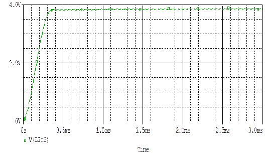
The Buck converter Output:
The Buck converter Output
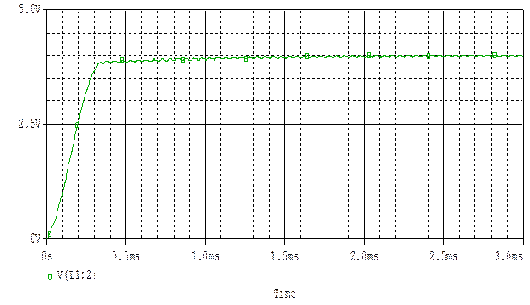
(1) Rejection of Input Variation
Rejection of Input Variation
(2) Output follows the control Reference:
Output follows the control Reference
Variation of Load:
Normal output at load 150 ohm.
Normal output at load 150 ohm
If we Change the load 150ohm to 200ohm than the output
Change the load 150ohm to 200ohm than the output
METHODOLOGY:
  1. Theoretical study and analysis of One cycle control technique .
  2. Simulate the One cycle control of Buck converter circuit with ORCAD 9.2.
  3. Collect the necessary components.
  4. Test each portion of circuit individually.
  5. Implementation the One cycle control of Buck converter circuit practically.
Experimental Setup
Experimental Setup
Opto-coupler wave Shape
Flip-flop output waveform
Inverted amplifier output
Buck Converter
Buck Converter
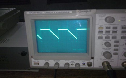
Integrator output wave shape:
Integrator output wave shape
Comparator Output
Comparator Output
Future Works:
The One-Cycle Control technique will be applied for the following type of Switches.
  1. Constant ON-time switch.
  2. Constant OFF-time switch
  3. Variable switch.
CONCLUSION:
converters with One Cycle Control are capable of rejecting the power source perturbations completely the average value of the switched variable at the switch output node is able to follow the control reference within one cycle. The One-Cycle Control concept is straightforward and its implementation circuits are simple, yet it provides excellent control.
REFERENCE:

  1. One-Cycle Control of Switching Converters. Keyue M. Smedley, Member, IEEE, and

Slobodan Cuk, Senior Member, IEEE.
  • An Integrated One-Cycle Control Buck Converter With Adaptive Output and Dual Loops for Output Error Correction. Dongsheng Ma, Member, IEEE, Wing-Hung Ki, Member, IEEE, and Chi-Ying Tsui, Member, IEEE.
  • One cycle control of three-phase VAR compensators and active power filters. Sandeep Bala (99007013) Department of Electrical Engineering, Indian Institute of Technology, Bombay, April 2003.
  • Keyue Ma Smedly. “Control Art of Switching Converter” California Institute of Technology, Pasadena, California, June 21, 1990.
  • Submitted by Ratan Kanti Das and Sufal Chandra Dey.

    Design of a Converter for producing a fixed valued AC from a variable AC Supply

    Presentation on Design of a Converter for producing a fixed valued AC from a variable AC Supply.

    Now a day a major problem of world is the scarcity of source of power production. We can generate power from various sources such as solar energy, wind energy, tidal power etc. But many of these sources cannot give a continuous flow of fixed amplitude and frequency output. Generally there are a few machines invented till now, that can be operated with variable fluctuating voltage input. For household or industrial application purpose, we are bound to use fixed ac voltage input. If we try to use this variable ac voltage as input to our regular usage machinery, such as lamps, fans, TV etc. then it would cause severe damage to our instruments. However, those facts of these machines necessitate efficient conversion system to operate their loads. So it is important firstly to convert this variable ac to a fixed dc. The power converter, positioned between the generator and the grid, transforms the variable-frequency ac to fixed dc and then to fixed ac. The total power output of the generator is combined by the converter (total conversion). Our thesis concerns a small range of this conversion system using available devices. In this thesis we have presented a low cost variable ac to fixed ac system with construction and details description of various parts.
    Objectives
    The objectives of this effort are-
    1. To convert variable ac input to fixed dc output through electronic converter circuit.
    2. To simulate that circuit with ‘p-spice’.
    3. To analyze the performance parameters of the designed circuitry.             
    Scope of works
    1. Set and Specify the aims of the objective.
    2. Have a clear idea about the possible outcome.
    3. Divide the whole design into small groups –
      -Generation of the variable alternating current.
      -Transformation of the variable frequency alternating current to a fixed valued direct current.
    4. Simulate that Generation circuit using electrical simulation software ‘p-spice’.
    5. Observe the output of that Generation circuit using electrical simulation software ‘p-spice’.
    6. To design and simulate the Converter.
    7. To observe the output of that circuit.
    Design steps
    1. Source Section
    2. Filtering Section
    3. Transformer Section
    4. Rectifier Section
    5. Capacitor input filter Section
    6. Inverter Section
    Schematic diagram of multiplier circuit
    Schematic diagram of multiplier circuit
    Voltage Wave shapes of input and variable ac output
    Voltage Wave shapes of input and variable ac output
    Current Wave shapes of variable ac output
    Current Wave shapes of variable ac output
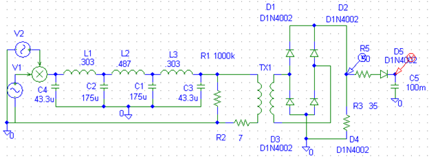
    Schematic diagram of Low pass filter circuit
    Schematic diagram of Low pass filter circuit
    Voltage Wave shapes of input and output of low pass filter
    Voltage Wave shapes of input and output of low pass filter
    Schematic diagram of Transformer circuit
    Schematic diagram of Transformer circuit
    Wave shapes of input and output of transformer
    Wave shapes of input and output of transformer
    Schematic diagram of rectifier circuit
    Schematic diagram of rectifier circuit
    Voltage Wave shapes of input and output of rectifier circuit
    Voltage Wave shapes of input and output of rectifier circuit
    Performance analysis of rectifier
    1. Vin =100.01V
    2. Vout = 98.975V
    3. η = 81%
    4. FF = 1.11
    5. RF = 0.482 = 48.2%
    6. PF = .707
    Schematic diagram of Capacitor input filter circuit
    Schematic diagram of Capacitor input filter circuit
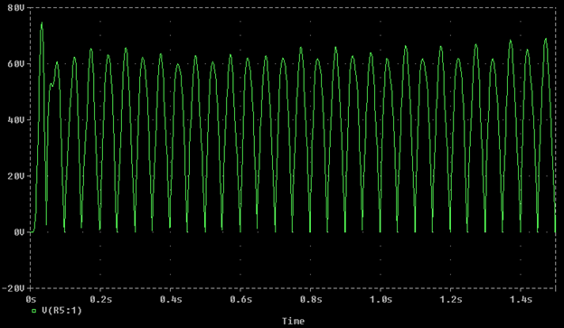
    Voltage Wave shapes of input of Capacitor input filter circuit
    Voltage Wave shapes of input of Capacitor input filter circuit
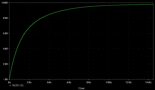
    Voltage Wave shapes of output of Capacitor input filter circuit
    Voltage Wave shapes of output of Capacitor input filter circuit
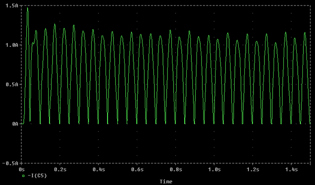
    Current Wave shapes of output of Capacitor input filter circuit
    Current Wave shapes of output of Capacitor input filter circuit
    Schematic diagram of Square wave inverter circuit
    Schematic diagram of Square wave inverter circuit
    Voltage Wave shapes of input and output of Square wave inverter circuit
    Voltage Wave shapes of input and output of Square wave inverter circuit
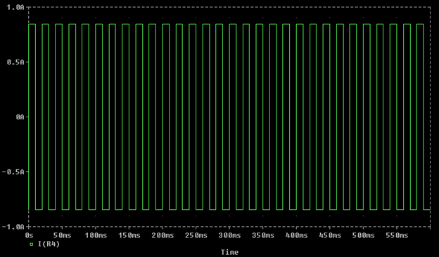
    Current Wave shapes of output of Square wave inverter circuit
    Current Wave shapes of output of Square wave inverter circuit

    Performance analysis of inverter
    1. Vs = 85 V
    2. R = 100 Ω
    3. The output power, Po =72.25 W
    4. THD =48.41 %
    5. DF =5.33 %
    6. LOH, V3 =25.51 V
    7. HF3 =33.33 %
    8. DF3 =3.704 %
    9. The load power, Po = 69.372 W
    10. The fundamental output power, Po1 = 58.568 W
    11. Power due to non-sinusoidal voltages and currents, p = 69.364 W
    12. The volt-ampere, Va = 69.364 volt-amperes
    13. P. F = 1
    Drawbacks
    A high valued capacitor is used here, hence the charging time constant of the capacitor is very high. The analog multiplier used in this simulation can be replaced by digital ICs such as AD633, ADL5390 etc. but those IC s have mw power ratings. As the conversion system is continuously connected to the supply system and MOSFETs are forced to conduct one after another, they may be heated which can destroy the MOSFET.
    Conclusion
    In this thesis we tried our best to represent the basic description of different section so as one can get basic idea about its constructional details. We describe it step by step to get fine concept about the system. At first we provide theoretical description about the system. Then we discussed about the constructional details and mention the sections where any interested person can develop the system in future.
    References
    1. Muhammad H. Rasid, “Power Electronics-Circuits, Devices and Application”, Prentice Hall of India Private Limited, New Delhi-110001, Second Edition
    2. Joseph Vithayathil, “Power Electronics- Principles and Applications”, McGraw-Hill, Inc., New York, International Edition.
    3. G. R. Nagpal “Power Plant Engineering”, Khanna publications, Delhi-110006, Fifteenth Edition
    4. Malvino, “Electronic Principles”, Tata McGraw-Hill Publishing Company Limited, New Delhi, Sixth Edition.
    5. Robert F. Coughlin and Fredrick F. Driscoll, “Operational Amplifiers and Linear Integrated Circuits”, Prentice Hall of India Private Limited, New Delhi-110001, Fourth Edition
    6. Bimal K. Bose, “Modern Power Electronics and AC Drives”, Prentice Hall of India Private Limited, New Delhi-110001, International Edition
    7. P. C. Sen, “Power Electronics”, Hall of India Private Limited, New Delhi-110001, International Edition
    Submitted BY: PINKY DUTTA and TAHSIN KARIM
    Digg This