Power Semiconductor Devices

More on this category »

Latest Post

Design & Implementation of Color Sensor

Presentation on Design & Implementation of Color Sensor.

Introduction
Light is a physical phenomenon.When the components of light are absorbed or transmitted in different proportions by an object, color occurs. The color of an object is apparent only when light strikes the object. For color to be perceived, the viewer must have blue, green, and red receptors. Depending upon its chemical make-up, matter has the ability to absorb, reflect or transmit visible light.
When all the components of visible light are absorbed by matter, the object is said to be black.On the other hand, if all the components of visible light are reflected or transmitted by the object, the object is considered white or clear. The visible light spectrum is a small part of the electro-magnetic spectrum. The visible spectrum has a wavelength range of about 380 to 740 nm. Human eye can perceived only the visible light.
Wavelength & frequency interval of different colors

Color Name
Wavelength Interval
nm
Frequency Interval
THz
Violet
380-450
668-789
Blue
450-495
606-668
Green
495-570
526-606
Yellow
570-590
508-526
Orange
590-620
484-508
Red
620-750
400-484
Objectives

The main objective of our project is to detect the color of an object. Our target is to detect ten colors.The target colors are Black, Green, Red, Blue, Yellow, Magenta, Yellow-lemon,Pink,
Gray, White.
To relate color system wherein color purity and mixings is identified perfectly and is independent of human observations or subjective judgments.
Possible Outcome

To detect the color of an object with high precision even under varying environment conditions, such as fluctuations in the ambient temperature or variations of incidence light on the object to be measured.
Experimental Design

A color sensor includes a light receiving element for receiving the light from an object(target) illuminated by the lights from the light emitting sources and a circuit arrangement for producing output signals representing the color of the object.
Experimental Design

Design & Implementation of Color Sensor
Op-amp

The op-amp is basically a differential amplifier having a large voltage gain, very high input impedance and low output impedance. Most of the time operational amplifiers are used to compare voltages of unequal magnitudes. They are called ``operational'' amplifiers, because they can be used to perform arithmetic operations (addition, subtraction, multiplication) with signals.
Op-amp Circuit Notation

Op-amp
V + : non-inverting input
V- : inverting input
Vout : output
Vs+: positive power supply
Vs-: negative power supply
Pin Connection of LM741

Pin Connection of LM741
Analog-to-digital converter (ADC)

An analog-to-digital converter (A/D) takes an analog voltage or current and after a certain amount of time it produces a digital output code that represents the analog input.
Simply, an analog-to-digital converter is a device which converts continuous signals to discrete digital numbers.

General Block Diagram (ADC)

General Block Diagram (ADC)

Pin diagram & free running connection

Pin diagram & free running connection
Pin diagram of ADC0804

Pin diagram of ADC0804
Free running connection

Microcontroller

Microcontroller is a programmable integrated circuit which contains Processor, memory and input/output functions in a single chip. It is a microprocessor emphasizing high integration. In contrast to a general-purpose microprocessor, the microcontroller integrates additional elements such as read write memory for data storage, read-only memory for program storage, EEPROM for permanent data storage, peripheral devices, and input/output interfaces.
Pin diagram (PIC16F84A)

Pin diagram (PIC16F84A)
Pin function

Pin diagram (PIC16F84A)
Circuit Diagram

Color Sensor circuit diagram

Color Sensor circuit diagram
Program

TRISA = 0
TRISB = 255
Dim a As Byte
PORTA = 0
WaitMs 10
main:
PORTA = 0
a = PORTB
If a < 11 Then PORTA = 1 '//Black
If a > 6 Then
If a < 27 Then PORTA = 2 '//Blue
Endif
If a > 26 Then
If a < 31 Then PORTA = 3 '//green
Endif
If a > 39 Then
If a < 44 Then PORTA = 4 ''// Pink
Endif
If a > 44 Then
If a < 50 Then PORTA = 5 '//Red
Endif
If a > 49 Then
If a < 57 Then PORTA = 6 '//Megenta
Endif
If a > 56 Then
If a < 63 Then PORTA = 7 '// White
Endif
If a > 64 Then
If a < 73 Then PORTA = 8 '//Yellow
Endif
If a > 89 Then
If a < 93 Then PORTA = 9 '//Gray
Endif
If a > 92 Then
If a < 96 Then PORTA = 10 '//Yel+lem
WaitMs 200
Goto main
Result

Our project is designed for detection of ten colors. But we have detected eight colors successfully. The detected eight colors are red, green, yellow, yellow-lemon, pink, gray, black & white.
Error

We can’t detect two colors. The colors are blue & magenta. This two colors are overlapped with green & red.
Limitation
  1. The major limitation of our project is that it can’t detect the object which contains number of colors.
  2. One limitation of this project is that it can’t display the color name. But it is possible to display the color name with the help of LCD display by proper programming.
  3. Our blue sensor can’t work properly. So we can’t detect the blue color as well as other color.
  4. We can’t filter the color perfectly.

Future study & improvement

  1. To display the detected color name.
  2. To increase the number of detected color.
  3. To detect number of colors even exist as a narrow strip within the object.
  4. Sort objects by color
Reference
  1. “Digital Systems Principles and Applications” By, Ronald J. Tocci, Neal S. Widmer & Gregory L. Moss
  2. “Digital Logic and Computer Design” By, M. Morris Mano
  3. “Operational Amplifiers and Linear Integrated Circuits” , Sixth edition By, Robert F. Coughlin and Frederick F. Driscoll
Submitted By Anup Kumar Das and Prashanta Kumer Sarker

Protective Relaying Principles and Applications

Power Electronic Control in Electrical Systems

Pulse-width modulated (PWM) VSCs followed by Three-level three-phase NPC VSC

Other multilevel converter topologies

Single-phase full-bridge NPC VSC

Single-phase half-bridge neutral-point-clamped (NPC) VSC

Conventional three-phase six-step VSC

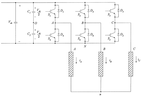
The conventional three-phase six-switch VSC is shown in Figure 6.32. It consists of six switches S1-S6 and six antiparallel diodes D1-D6. The number indicates their order of being turned on. A fictitious neutral (o) as a mid-point is also included although in most cases is not available. However, when the converter under consideration is used as an active filter in the case of a four-wire three-phase system, this point (o) is used to connect the fourth-wire. This case will be discussed further in later parts.

The three converter legs are controlled with a phase-shift of 120o between them. The basic way to control the three-phase six-switch VSC is to turn on each switch for half of the period (1800) with a sequence 1, 2, 3, . . . as they are numbered and shown in Figure 6.32.

Conventional three-phase six-switch VSC

Fig. 6.32  Conventional three-phase six-switch VSC.


The operation of the converter can be explained with the assistance of Figure 6.33. Specifically, the control signals for each of the six switches are shown in Figure 6.33(a). Clearly, each switch remains on for 1800 and every 600 a new switch is turned on and one of the previous group is turned off. At any given time therefore, one switch of each leg is on. Assuming that the fictitious mid-point (0) is available, three square-type waveforms for the voltages vAO, vBO, and vCO can be drawn as shown in Figure 6.33(b). Each of the voltage waveforms has two peak values of Vdc/2, and -Vdc/2, and they are displaced by 120o from each other.

From the three waveforms vAO, vBO, and vCO, the line-to-line voltage waveforms can be drawn since

image
The three resultant line-to-line voltage waveforms are then shown in Figure 6.33(c). It is clear that each waveform takes three values (Vdc, 0, -Vdc) and there is a 120o phase-shift between them. These waveforms have a 60o interval when they are zero for each half of the period, a total of 120o per period. As explained earlier, each leg can handle current in both directions at any time, since either the turned on switch or the antiparallel diode of the other switch can be the conducting element depending upon the polarity of the output line current.

The potential of the load neutral point (n) shown in Figure 6.32 with respect to the mid-point of the DC bus (0) is drawn in Figure 6.33(d). It can be seen that such a waveform has frequency three times the output frequency and the two peak values are between Vdc/6 and -Vdc/6. Finally, the line-to-load neutral point (n) voltage waveform is illustrated in Figure 6.33(e). Such a voltage waveform has two positive values (Vdc/3 and 2Vdc/3) and two negative ones (-Vdc/3 and -2Vdc/3).

Key waveforms of the three-phase six-step VSC circuit operation


Fig. 6.33 Key waveforms of the three-phase six-step VSC circuit operation. (a) control signals for switches S1, S2, S3, S4 ,S5 , S6; (b) voltage waveforms vAO, vBO, and vCO; (c) output line-to-line voltage waveforms vAB, vBC, vCA ; (d) voltage waveform between the load neutral point (n) and the DC bus mid-point (0); (e) voltage waveform between the line point A and the load neutral point n; (f) harmonic spectrum of the line-to-DC bus mid-point; and (g) harmonic spectrum of the line-to-line voltage vAB.


The harmonics of the various waveforms can be calculated using Fourier series. The fundamental amplitude of the voltage waveforms vAO, vBO, and vCO is

image

where h is the order of the harmonic.
For the line-to-line voltage waveforms vAB, vBC, and vCA  then the fundamental amplitude is

image
and therefore the rms value of the fundamental component is then
image

Similarly, the amplitude of the harmonic voltages is

image

The rms value of the line-to-line voltage including all harmonics is

image


The  normalized  spectrum  of  the  line-to-DC  bus  mid-point  and  the  line-to-line voltage waveforms are plotted in Figures 6.33(f) and (g) respectively. It can be seen that the voltage waveforms vAO, vBO, and vCO contain all odd harmonics. The load connection as shown in Figure 6.32 does not allow 3rd harmonic and all multiples to flow, and this is confirmed with the spectrum of the line-to-line voltage waveform vAB where 3rd, 9th and 15th harmonics are eliminated as shown in Figure 6.33(g).
previous Single-phase full-bridge VSC

next Single-phase half-bridge neutral-point-clamped (NPC) vSC

Single-phase full-bridge VSC

In this section we will examine in detail the single-phase full-bridge VSC. Its power circuit is shown in Figure 6.26. It consists of two identical legs like the half-bridge single-phase converter (Figure 6.23) discussed in Section 6.3.1. Specifically, there are four switching elements (S1, S2, S3, S4), four antiparallel diodes (D1, D2, D3, D4) and a DC bus voltage source Vdc that can be a single capacitor. The other leg provides the return path for the current this time and the DC bus mid-point does not need to be available to connect the load. The output voltage v0 appears across the two points A and B as shown in Figure 6.26.

The control restriction discussed for the single-phase half-bridge topology (Figure 6.23) applies to this converter as well. Clearly the control signals for the switch pairs (S1, S2) and (S3, S4) must be complementary to avoid any bridge destruction due to shoot through of infinite current (at least theoretically).

There are two control methods for this topology. The first one treats the switches (S1, S4) and (S2, S3) as a pair. This means that they are turned on and off at the same time and for the same duration. For square-wave operation the switches S1 and S4 are on for half of the period. For the other half, the pair of S2, S3 is turned on. Like the single-phase half-bridge VSC, the direction of the output current i0 determines the conduction state of each semiconductor.

When the two switches S1 and S4 are turned on, the voltage at the output is equal to the DC bus voltage Vdc. Similarly, when the switches S2 and S3 are turned on the output voltage is equal to - Vdc. Such circuit operation is illustrated in Figure 6.27.

In the first case, when the direction of the output current io is positive as shown in Figure 6.26, the current flows through switches S1 and S4 and the power is transferred from the DC side to the AC one (t4 < t < t5). When the current becomes negative, although the switches S1 and S4 are turned on, the diodes D1 and D4 conduct the current and return power back to the DC bus from the AC side (t3 < t < t4). For the other half of the period, when the switches S2 and S3 are turned on and the current is positive, the diodes D2 and D3 conduct (t1 < t < t2). In this

Single-phase full-bridge VSC

Fig. 6.26 Single-phase full-bridge VSC.

Key waveforms of the single-phase full-bridge VSC circuit operation

Fig. 6.27 Key waveforms of the single-phase full-bridge VSC circuit operation. (a) output voltage V0 = VAB; (b) output current i0; (c) input DC bus current id; (d) harmonic spectrum of the output voltage V0 = VAB; (e) harmonic spectrum of the output current i0; and (f) harmonic spectrum of the input DC bus current id.

instance, power is transferred also back to the DC side from the AC side. Finally, when the current is negative, the switches S2 and S3 carry the current and assist the converter to transfer power from the DC bus to the AC side (t2 < t < t3). In summary, there are four distinct modes of operation for this converter when the control method shown in Figure 6.27 is employed (two inverter modes and two rectifier modes). Simply said, at all times two switches are turned on and the legs are controlled in a synchronized way.

The output voltage v0 = vAB is shown in Figure 6.27(a). The output current i0 and the input DC current id are also plotted in Figures 6.27(b) and (c) respectively. Similarly, like the case of the half-bridge topology, the square-wave generated across the AC side includes all odd harmonics and being a single-phase system, the third harmonic is also present (Figure 6.27(d)). These harmonics when reflected back to the DC side source include all even harmonics (Figure 6.27(f).

Quadrants of operation of the single-phase full-bridge VSC

Fig. 6.28 Quadrants of operation of the single-phase full-bridge VSC.

The fundamental component of the output voltage v0 waveform has an amplitude value of

{\left( {{{\hat V}_0}} \right)_1} = {\left( {{{\hat V}_{AB}}} \right)_1} = \frac{{4 \cdot {V_{dc}}}}{\pi }                (6.20)

And its various harmonics are given by

{\left( {{{\hat V}_0}} \right)_h} = {\left( {{{\hat V}_{AB}}} \right)_h} = \frac{{4.{V_{dc}}}}{{\pi .h}} = \frac{{{{\left( {{{\hat V}_0}} \right)}_1}}}{h}{\rm{               }}h = 3,5,7,9,.....

where h is the order of the harmonic.

The converter is capable of operating in all four quadrants of voltage and current as shown in Figure 6.28. The various modes and their relationship to the switching and/or conduction state of the semiconductors are also summarized in Table 6.4 for further clarity. The phase relationship between the AC output voltage and AC output current does not have to be fixed and the converter can provide real and reactive power at all leading and lagging power factors. However, the converter itself cannot control the output voltage if the DC bus voltage Vdc remains constant. There is a need to adjust the level of the DC bus voltage if one wants to control the rms value of the output voltage v0.

There is however a way to control the rms value of the fundamental component of the output voltage as well as the harmonic content of the fixed waveform shown in Figure 6.27(a). In this method, the control signals of the two legs are not

Table 6.4 Modes of operation of the single-phase full-bridge VSC

Modes of operation of the single-phase full-bridge VSC

synchronized  in  any  way  and  the  switches  are  not  treated  as  pairs  like  previously. For the safe  operation  of  the  converter,  the  control  signals  between (S1 and S2) and (S3 and S4) must be complementary. In this case, there is a phase- shift between the two legs and this way a zero volts interval can appear across the output.

For instance, if switches S1 and S3  are turned on at the same time, the output voltage (vAB) will be zero. The current in the case of other than unity power factor must keep flowing. There is no power exchange between the DC side and the AC one (free-wheeling mode). If the current is positive, the current flows through S1 and D3. If the current is negative, it flows through D1 and S3. Similarly, when the two bottom switches S2 and S4 are turned on at the same time, the output voltage (vAB) is zero and the output current once again determines which element conducts and allows the output current to continue flowing. Specifically, if the current is positive, the diode D2 and the switch S4 are conducting. In the case that the current is negative, the switch S2 and diode D4 provide a path for the output current. These extra modes of operation for the single-phase full-bridge topology (Figure 6.26) are also included in Table 6.4 as the free-wheeling modes.

For a given phase-shift (a degrees) between the control signals of the two legs, the waveforms are shown in Figure 6.29. It is clear that the output voltage waveform is a three-level one, being able to have the values of Vdc, 0 and -Vdc as shown in Figure 6.29(a). The control signals are shown in Figures 6.29(b)-(d). It is also clear that between the top and bottom switches of each leg complementary control signals are used. It should be noted that for α = 0, the output voltage becomes similar to the previously presented control method (square-wave, Figure 6.27(a)).


The output voltage vo  (vAB) is shown in Figure 6.30(a) along with the output current io and the DC bus current id in Figures 6.30(b) and (c) respectively. Therefore, by controlling the phase-shift between the two legs (α degrees), the rms value of the fundamental component can be controlled. The amplitude of all odd harmonics, as shown in Figure 6.30(d) for the output voltage, can also be controlled. The output current has only a fundamental component as shown in Figure 6.30(e), where the DC bus current has a DC component and all even harmonics as shown in Figure 6.30(f).

Key  waveforms  of  the  single-phase  full-bridge  phase-shifted  controlled  VSC circuit  operation


Fig.  6.29  Key  waveforms  of  the  single-phase  full-bridge  phase-shifted  controlled  VSC circuit  operation. (a)  output  voltage  vo = vAB;  (b)  control  signal  for  switch  S1 ;  (c)  control  signal for  switch  S2;  (d)  control signal for switch S3; and (e) control signal for switch S4.
Key waveforms of the single-phase full-bridge phase-shifted controlled VSC circuit operation

Fig. 6.30 Key waveforms of the single-phase full-bridge phase-shifted controlled VSC circuit operation. (a) output voltage vo = vAB; (b) output current io; (c) DC bus current id; (d) harmonic spectrum of the output voltage vo = vAB; (e) harmonic spectrum of the output current io; and (f) harmonic spectrum of the input DC bus current id.
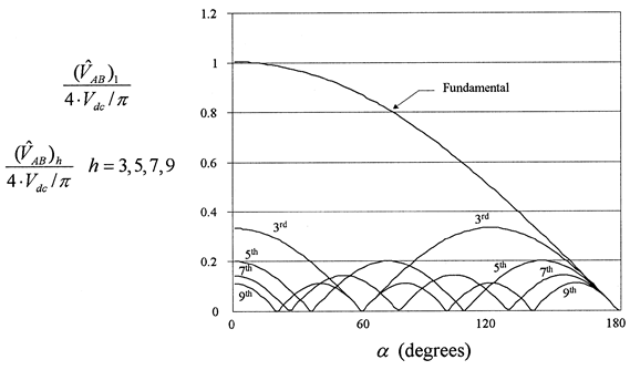
Normalized amplitudes of fundamental and harmonics for the phase-shifted output voltage as a function of α (zero volts interval in degrees)


Fig. 6.31  Normalized amplitudes of fundamental and harmonics for the phase-shifted output voltage as a function of α (zero volts interval in degrees).


For a given zero interval α in degrees, as shown in Figures 6.29(a) and 6.30(a), the amplitude of the fundamental and harmonics are as follows

image


where h is the order of the harmonic.
When α = 0  the converter operates as a  square-wave one  (Figure  6.27). The normalized amplitude of the fundamental and the most significant harmonics, i.e. 3rd, 5th, 7th and 9th to the output of the square-wave converter as a function of α, are plotted in Figure 6.31.

previous Single-phase half-bridge VSC

next Conventional three-phase six-step VSC

Single-phase half-bridge VSC

Let us consider first the simplest and basic solid-state DC-AC converter, namely the single-phase half-bridge VSC. Figure 6.23 shows the power circuit. It consists of two switching devices (S1 and S2) with two antiparallel diodes (D1 and D1) to accommodate the return of the current to the DC bus when required. This happens when the load power factor is other than unity. In order to generate a mid-point (0) to connect the return path of the load, two equal value capacitors (C1 and C2) are connected in series across the DC input. The result is that the voltage Vdc is split into two equal sources across each capacitor with voltage of Vdc/2. The assumption here is that the value of the capacitors is sufficiently large to ensure a stiff DC voltage source. This simply means that their voltage potential remains unchanged during the operation of the circuit. This also means that the potential of the mid-point (0) is constant with respect to both positive and negative DC bus rails at all times (Vdc/2) and - Vdc/2 respectively).
Single-phase half-bridge VSC
Fig. 6.22 Single-phase half-bridge VSC.
Let us now examine the operation of this circuit. It can be explained in combination with Figure 6.24. The two control signals for turning on and off the switches S1 and S2 are complementary to avoid destruction of the bridge. This would happen due to the throughput of high current coming from the low impedance DC voltage sources, if both switches were turned on simultaneously. When the switch S1 is turned on (t3 < t < t5), the output voltage v0 = vAO is equal to the voltage Vdc/2 of the capacitor C1. The mode of operation of the switching block (S1 and D1) is then controlled by the polarity of the output current i0. If the output current is positive, with respect to the direction shown in Figure 6.23, then the current is flowing through switch S1 (t4 < t < t5, Figure 6.24). If the output current is negative, the diode D1 is conducting, although switch S1 is turned on (t3 < t < t4). Similarly, if the switch S2 is turned on (t1 < t < t3), the output voltage is equal to the voltage Vdc/2 of the capacitor C2 with the polarity appearing negative this time. The output current i0 once again determines the conduction state of the switch and diode. If the output current is positive, the diode D2 is conducting (t1 < t < t2). If the output current is negative, the current flows through switch S2 (t2 < t < t3). Such states of switches and diodes are clearly marked in the waveforms of Figure 6.24 for the various time intervals. The modes of operation of the half-bridge single-phase VSC are also summarized in Table 6.3.
Figure 6.24(a) shows the output voltage waveform v0 = vA0 generated by the converter operation as previously explained. Due to the square-wave generated by the converter, the output voltage waveform is rich in harmonics. Specifically, as shown in Figure 6.24(c) all odd harmonics are present in the spectrum of the output voltage. The fact that the converter cannot control the rms value of the output voltage waveform at fundamental frequency is also a limitation. A separate arrangement must be made to vary the DC bus voltage Vdc in order to vary and control the output voltage v0.
Key waveforms of the single-phase half-bridge VSC circuit operation
Fig. 6.24 Key waveforms of the single-phase half-bridge VSC circuit operation. (a) output voltage V0 = VA0; (b) output current i0; and (c) harmonic spectrum of the output voltage V0 = VA0.
Single-phase half-bridge VSC
The amplitude of the fundamental component of the output voltage square-wave v0 shown in Figure 6.24(a) can be expressed using Fourier series as follows
{({\hat V_0})_1} = {({\hat V_{A0}})_1} = \frac{{4.{V_{dc}}}}{{1.\pi }}                 (6.18)
The amplitude of all the other harmonics is given by
{({\hat V_0})_h} = {({\hat V_{A0}})_h} = \frac{{4.{V_{dc}}}}{{2.\pi .h}} = \frac{{{{({{\hat V}_0})}_1}}}{h}{\rm{        }}h = 3,5,7,9,......           (6.19)
where h is the order of the harmonic.
quadrants of operation of the single-phase half-bridge VSC
Fig. 6.25 quadrants of operation of the single-phase half-bridge VSC.
The converter discussed here operates in all four quadrants of output voltage and current as shown in Figure 6.25. There are two distinct modes of operation associated with the transfer of power from the DC to the AC side. When the power flows from the DC bus to the AC side, the converter operates as an inverter. The switches S1 and S2 perform this function. In the case that the power is negative, which means power is returned back to the DC bus from the AC side, the converter operates as a rectifier. The diodes D1 and D1 perform this function.
The capability of the converter to operate in all four quadrants (Figure 6.25)
means that there is no restriction in the phase relationship between the AC output voltage and the AC output current. The converter can therefore be used to exchange leading or lagging reactive power. If the load is purely resistive and no filter is attached to the output the diodes do not take part in the operation of the converter and only real power is transferred from the DC side to the AC one. Under any other power factor, the converter operates in a sequence of modes between a rectifier and an inverter. The magnitude and angle of the AC output voltage with respect to the AC output current control in an independent manner the real and reactive power exchange between the DC and AC sides.
This converter is also the basic building block of any other switch-mode VSC.
Specifically, the combination of the switching blocks (S1 and the antiparallel diode D1) and (S2 and D2) can be used as a leg to build three-phase and other types of converters with parallel connected legs and other topologies. These types of converters will be described later.
previous Voltage-source converters (VSCs) and derived controllers
next Single-phase full-bridge VSC