previous GATE PULSE GENERATION PROCESS OF THREE-PHASE FULL WAVE RECTIFIER
6.1 RESULT OF THE THREE-PHASE INVERTER
Here we add our result and images of hardware with corresponding wave shapes shown in oscilloscope screen.
6.1.1 CIRCUIT AND HARDWARE

6.1.2 PULSES FROM THE MICROCONTROLLER OUTPUT




Current Output:



REFERENCES
[1] Digital Power Electronics and Applications - Fang Lin Luo, Hong Ye, Muhammad Rashid (art-5.1, page-142)
[2] Power Electronics Design: A Practitioner’s Guide-Keith H. Sueker (Chapter 9: Rectifiers and Converters)
[3] Digital Power Electronics and Applications - Fang Lin Luo, Hong Ye, Muhammad Rashid (art-6.1)
[4] POWER ELECTRONICS HANDBOOK - MUHAMMAD H. RASHID (art-12.1)
[5] POWER ELECTRONICS HANDBOOK - MUHAMMAD H. RASHID (art-13.1)
[6] POWER ELECTRONICS HANDBOOK - MUHAMMAD H. RASHID (art-13.10)
[7] Digital Power Electronics and Applications - Fang Lin Luo, Hong Ye, Muhammad Rashid (art-6.1)
[8] Digital Power Electronics and Applications - Fang Lin Luo, Hong Ye, Muhammad Rashid (art- 6.1.1, 6.1.2)
[9] Version 2 EE IIT, Kharagpur - Module 5 DC to AC Converters (Lesson 35 3-Phase Voltage Source Inverter with Square Wave Output)
[10] Digital Power Electronics and Applications - Fang Lin Luo, Hong Ye, Muhammad Rashid (art-6.1.3)
[11] Digital Power Electronics and Applications - Fang Lin Luo, Hong Ye, Muhammad Rashid (art-5.3, 5.4, 5.5, 5.6)
[12] Module: EE2A2 Embedded Microprocessor Systems – James Grimbleby (School of System Engineering – Electronic Engineering)
[13] MICROCHIP - PIC16F72 Data Sheet
[14] LM124, LM224 - LM324 - Data Sheet
6.1 RESULT OF THE THREE-PHASE INVERTER
Here we add our result and images of hardware with corresponding wave shapes shown in oscilloscope screen.
6.1.1 CIRCUIT AND HARDWARE

Figure 6.1: Real circuit connection in bread-board
6.1.2 PULSES FROM THE MICROCONTROLLER OUTPUT
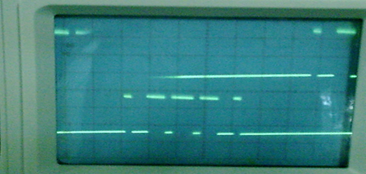
The pulses we get from the microcontroller is enough to run the IGBT’s. The high magnitude of the pulses is 4.98 volts when it is connected to the gates of the IGBT’s.

Figure 6.2: Phase 1 and phase 2

Figure 6.3: Phase 1 and phase 3

Figure 6.4: Phase 2 and phase 3(same as figure 6.2)

Figure 6.5: phase 1 and phase 1΄

Figure 6.6: Phase 2 and phase 2΄

Figure 6.7: Phase 3 and phase 3΄
6.1.3 THE IGBT MODULE OUTPUTSCurrent Output:
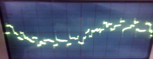
Here 3 current wave shapes we get from phase A are shown in 3 different time scale in figure 6.8, figure 6.9 and figure 6.10 respectively. The loads are R-L loads.
Figure 6.8: Current at phase A (low time scale)

Figure 6.9: Current at phase A (high time scale)

Figure 6.10: Current at phase A (medium time scale)
Voltage Output:
We have use about 40 v at the DC input terminals.We get line to nutral balanced rms voltage 18.7 volt from multimeter and the line to line rms voltage is about 27 volt.The output voltage wave form of phase A is shown in figure 6.11.
Figure 6.11: Voltage of phase A
Figure 6.12: Overall set up
6.2 RESULT OF THE CONTROLLED RECTIFIER
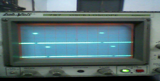
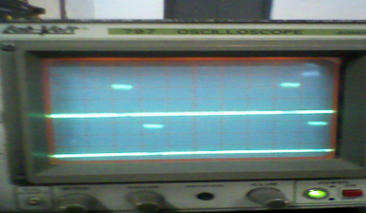
From the SCR control circuit we get the pulses shown in the figures from 6.13 to 6.18. The magnitude of the high states is 5 volts each. After applying this pulses we get about 18.72 volts dc for 4ms firing delay which is approximate with the built-in thyristor firing unit for which we get about 18 volt for the approximately the same delay angle. Using the smoothing inductance we have about 0.98 Ampere current flowing from the DC output terminal.
Figure 6.13: Thyristor 1 and Thyristor 2 gate pulses
Figure 6.14: Thyristor 1 and Thyristor 3 gate pulses

Figure 6.15: Thyristor 1 and Thyristor 4 gate pulses

Figure 6.16: Thyristor 1 and Thyristor 5 gate pulses

Figure 6.17: Thyristor 1 and Thyristor 6 gate pulses

Figure 6.18: Thyristor 6 and Thyristor 2 gate pulses
CONCLUSION
This was a challenge to us. We achieve a vast knowledge implementing this project. We learn clearly about the gate pulses and how this two converters work from this project. At first we try to implement this with MTS-86c. But we ware not able to run multiple loops in this. We slightly succeeded to generate square waves. With the square wave we can run the IGBT module but for more accuracy we tried to generate sine PWM. So we next try it with Microcontroller. Finally we succeeded to generate an accurate set of sine PWM from PIC16F72. Initially it was our out of knowledge and even now we are amateur about this. But it is not so tough to work with it if the loader is available, because the HEX code conversion is easier then the assembly language.
In case of SCR control pulses generation we face difficulties in the sensing the positive going pulses. It can be sensed easily by clocked flip-flop. At last we ware able to overcome this difficulties. To overcome this difficulties the HELP portions and the library of the MikroC language and its emulator was a great help.
The rise time and fall time of the pulses are very low. So this scheme described in this paper can be useful to any power module with medium range of power.
For the further extension it is recommended to define the delay used in the programs with symbols and then in case of inverter if all the delays can be multiplied with a factor the frequency of the generated sine wave and in case of controlled rectifier the initial delay (4 ms) can also be changed similarly.
Finally this project is helpful for us by making confident to face any kind of problems created in our real field of interest.REFERENCES
[1] Digital Power Electronics and Applications - Fang Lin Luo, Hong Ye, Muhammad Rashid (art-5.1, page-142)
[2] Power Electronics Design: A Practitioner’s Guide-Keith H. Sueker (Chapter 9: Rectifiers and Converters)
[3] Digital Power Electronics and Applications - Fang Lin Luo, Hong Ye, Muhammad Rashid (art-6.1)
[4] POWER ELECTRONICS HANDBOOK - MUHAMMAD H. RASHID (art-12.1)
[5] POWER ELECTRONICS HANDBOOK - MUHAMMAD H. RASHID (art-13.1)
[6] POWER ELECTRONICS HANDBOOK - MUHAMMAD H. RASHID (art-13.10)
[7] Digital Power Electronics and Applications - Fang Lin Luo, Hong Ye, Muhammad Rashid (art-6.1)
[8] Digital Power Electronics and Applications - Fang Lin Luo, Hong Ye, Muhammad Rashid (art- 6.1.1, 6.1.2)
[9] Version 2 EE IIT, Kharagpur - Module 5 DC to AC Converters (Lesson 35 3-Phase Voltage Source Inverter with Square Wave Output)
[10] Digital Power Electronics and Applications - Fang Lin Luo, Hong Ye, Muhammad Rashid (art-6.1.3)
[11] Digital Power Electronics and Applications - Fang Lin Luo, Hong Ye, Muhammad Rashid (art-5.3, 5.4, 5.5, 5.6)
[12] Module: EE2A2 Embedded Microprocessor Systems – James Grimbleby (School of System Engineering – Electronic Engineering)
[13] MICROCHIP - PIC16F72 Data Sheet
[14] LM124, LM224 - LM324 - Data Sheet


Thank you for article
ReplyDelete