previous 5 PULSE SINE PWM GENERATION FOR IGBT BASED INVERTER
5.1 WAVE SHAPE CONSIDERATION


Condition 1:
Condition 2:
3. After the output of the comparator goes low state to high it will start to generate the pulses.
5.3 DURATION OF LOGIC STATES

void main()
{
trisb=0b00000000; // Defining port B as output //
trisc=0b10000000; // Defining pin no. 7 of port C as input //
portb=0; // Initially hold the port B to idle //
check:
if(portc.f7==0) // Condition check for entering at ready state only for port C7 = 0 //
{
goto run; // Jump to ready state defined by run //
}
if(portc.f7==1) // Avoiding the initial high state //
{
portb=0; // Keeping the port B in idle for port C7 in high //
goto check;
}
run:
while(portc.f7==0)
{
asm nop;
}
if(portc.f7==1) // After the initial low and than high, entering the loop //
{
delay_ms(4); // Defined delay for the controlled rectifier //
while(1) // Infinite loop instruction //
{
portb=0b00000001; // Starts the logic conditions according to figure 5.8 //
delay_ms(1);
portb=0b00000000;
delay_us(2333);
portb=0b00100000;
delay_ms(1);
portb=0b00000000;
delay_us(2334);
portb=0b00000010;
delay_ms(1);
portb=0b00000000;
delay_us(2333);
portb=0b00001000;
delay_ms(1);
portb=0b00000000;
delay_us(2333);
portb=0b00000100;
delay_ms(1);
portb=0b00000000;
delay_us(2334);
portb=0b00010000;
delay_ms(1);
portb=0b00000000;
delay_us(2333);
}
}
}
5.5 FLOW CHART

5.6 CONNECTION DIAGRAM

5.1 WAVE SHAPE CONSIDERATION
Let us consider a three phase 50 Hz power to be rectified with e typical SCR module. The desired signals are shown in figure 5.1.
Figure 5.1: Three phase sine waves
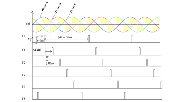
To generate desired gate pulses we have to sense the intersection points of the phase voltages. For this we need to consider figure 5.1 with a specific delay. Let the delay be α and in term of time it is 4 ms. Than according to the sequence of figure 5.2 we need the ideal gate pulses shown in figure 5.3.

Figure 5.2: Typical 3-phase thyristor rectifier

Figure 5.3: Desired gate pulses
We need the START point indecated in the figure 5.3. For this we have to use a comperator to sense the intersection point or the START point where the comperator will be turn high or low and this should be an input trigger of the microcontroller.
5.2 SENSING LOGIC DETERMINATION
Let us use a comperator with 2 input pins indicated by inverting and noninverting input and an output pin. If we connect the phase voltage as shown in figure 5.4 we will get the output pulses as shown in figure 5.5.

Figure 5.4: Typical comparator connection

Figure 5.5: Comparator output voltage
Form figure 5.5 we get the START point of figure 5.3. But there is a problem at the initial condition. Let see the figure 5.6 for two situations which can be correct or incorrect.
Figure 5.6: Different switch on conditions
5.2.1 STARTING CONDITIONSCondition 1:
Considering figure 5.6 if we switched on the power at point SW1 as indicated in the figure, the microcontroller senses a positive going pulse and start to generate the gate pulses from point SW1 instead of point p. It will generate a wrong pulse sequences.
Condition 2:
If we switched on the power at point SW2 as indicated in the figure 5.6, the microcontroller senses a zero state and start to generate the gate pulses from point q instead of point p. It will generate pulse sequences only accomplishing a delay starting from point p to q. This is not an error and no wrong sequences will be held.
5.2.2 PROGRAMMING LOGIC FOR STARTING
The program needs to start avoiding the error containing in condition 1. For this we have to check some conditions before the microcontroller started the loop for generating gate pulses. For this the microcontroller must check the following initial conditions.
1. If the output pulse of the comparator is initially in high state the microcontroller will d nothing.
2. Than it will check whatever the comparator output is high or low. If low it will be ready to generate pulses.3. After the output of the comparator goes low state to high it will start to generate the pulses.
5.3 DURATION OF LOGIC STATES
Rearranging the gate pulses on figure 5.3 we get simplified sequences as shown in figure 5.7. Assuming the duration of the thyristor in high state only for 1 ms we can conclude that between two consecutive high at two different gates all the gates will be in low states for 2.333 ms. These Logic states are shown with duration for each in figure 5.8.
Figure 5.7: Gate pulses with rearranged sequence

Figure 5.8: Gate logic states with corresponding durations
5.4 mikroC INSTRUCTION FOR MICROCONTROLLERvoid main()
{
trisb=0b00000000; // Defining port B as output //
trisc=0b10000000; // Defining pin no. 7 of port C as input //
portb=0; // Initially hold the port B to idle //
check:
if(portc.f7==0) // Condition check for entering at ready state only for port C7 = 0 //
{
goto run; // Jump to ready state defined by run //
}
if(portc.f7==1) // Avoiding the initial high state //
{
portb=0; // Keeping the port B in idle for port C7 in high //
goto check;
}
run:
while(portc.f7==0)
{
asm nop;
}
if(portc.f7==1) // After the initial low and than high, entering the loop //
{
delay_ms(4); // Defined delay for the controlled rectifier //
while(1) // Infinite loop instruction //
{
portb=0b00000001; // Starts the logic conditions according to figure 5.8 //
delay_ms(1);
portb=0b00000000;
delay_us(2333);
portb=0b00100000;
delay_ms(1);
portb=0b00000000;
delay_us(2334);
portb=0b00000010;
delay_ms(1);
portb=0b00000000;
delay_us(2333);
portb=0b00001000;
delay_ms(1);
portb=0b00000000;
delay_us(2333);
portb=0b00000100;
delay_ms(1);
portb=0b00000000;
delay_us(2334);
portb=0b00010000;
delay_ms(1);
portb=0b00000000;
delay_us(2333);
}
}
}
5.5 FLOW CHART

5.6 CONNECTION DIAGRAM

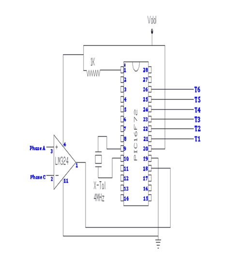
Figure 5.9: Connection diagram of PIC16F72 for SCR module.
next RESULT OVERVIEW OF THE INVERTER


No comments:
Post a Comment
Please wait for approval of your comment .......