Presentation GENERATION OF GATE PULSES WITH THE AID OF MICROCONTROLLER FOR VARIOUS POWER ELECTRONICS CONVERTERS
Objectives- To study about different types of gate pulses.
- To study the architecture of Microcontroller PIC16f72 and its application as a programmable gate pulse generator.
- To study the architecture of comparator LM 324 for using as sensing device for the triggering point of three phase sine wave.
- Generation of programmable gate pulses for driving a three phase IGBT module.
- Generation of programmable gate pulses for driving a typical SCR module.
- The main advantage of programmable gate pulses is the opportunity to change program according to the requirements.
- Same device can be used for different types of gate pulses.
- Controlling the abnormality of the power devices using feedback.
- Wide range of control over frequency.
A microcontroller typically includes-
- CPU (Central Processing Unit or the microprocessor)
- EEPROM / EPROM / PROM / ROM (Read Only Memory for the program code)
- RAM (Random, Access Memory for the program code)
- I /O (Input / Output) devices (serial, parallel, ADC, DAC etc.)
- Timers
- Interrupt controller
- Embedded Controller
- ADC
- Calculator
- PWM function generator

Application of Microcontroller
• Building control
- Access control• Industrial control
- Temperature sensing
- lighting
- Process control• Instrumentation
- Industrial instrumentation• Metering
- Handheld metering systems• Motor speed control
- AC motor control• Automotive
- DC motors
- Steppers
- LIN slave nodesOp-Amp LM324
- Body and convenience electronics
These circuits consist of four independent, high gain, internally frequency compensated operational amplifiers.They operate from a single power supply over a wide range of voltages. Operation from split power supplies is also possible and the low power supply current drain is independent of the magnitude of the power supply voltage.
Pin Diagram

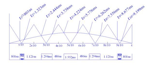
IGBT Gate Pulse Calculation


Solving equation above we get the value of t1 = 800.8429071 us
Logic States of PWM for Positive Half Cycle

Three Phase Representation in terms of Six Gate Signals

Sample Logic States with Duration for First 5 Conditions

Sample Program For First Two Durations
void main()
{
trisa = 0b00000000; // defining all the pins of port A are output pins //
trisb = 0b00000000; // defining all the pins of port B are output pins //
while(1) // infinite loop creation //
{
portb=0b00000001; // changing the states of RB0, RB1 and RB2 to 1, 0 and 0 respectively //
porta=0b00000010; // changing the states of RA0, RA1 and RA2 to 0, 1 and 0 respectively //
delay_us(405); // holding the above states of the pins for 405 microsecond //
portb=0b00000001; // changing the states of RB0, RB1 and RB2 to 1, 0 and 0 respectively //
porta=0b00000000; // changing the states of RA0, RA1 and RA2 to 0, 0 and 0 respectively //
delay_us(396); // holding the above states of the pins for 396 microsecond //
}
}
Block Diagram for IGBT Inverter

Connection Diagram for IGBT Inverter

Output Gate Pulses of Phase 2 and Phase 2΄

Combined Set of Wave Shapes

Gate pulses with rearranged sequence


mikroC Instruction for Controlled Rectifier
void main()
{
trisb=0b00000000; // Defining port B as output //
trisc=0b10000000; // Defining pin no. 7 of port C as input //
portb=0; // Initially hold the port B to idle //
check:
if(portc.f7==0) // Condition check for entering at ready state //
{
goto run; // Jump to ready state defined by run //
}
if(portc.f7==1) // Avoiding the initial high state //
{
portb=0; // Keeping the port B in idle for port C7 in high //
goto check;
}
run:
while(portc.f7==0)
{
asm nop;
}
if(portc.f7==1) // After the initial low and than high, entering the loop //
{
delay_ms(4); // Defined delay for the controlled rectifier //
while(1) // Infinite loop instruction //
{
portb=0b00000001; // Starts the logic conditions according to figure 5.8 //
delay_ms(1);
portb=0b00000000;
delay_us(2333);
portb=0b00100000;
delay_ms(1);
portb=0b00000000;
delay_us(2334);
portb=0b00000010;
delay_ms(1);
portb=0b00000000;
delay_us(2333);
portb=0b00001000;
delay_ms(1);
portb=0b00000000;
delay_us(2333);
portb=0b00000100;
delay_ms(1);
portb=0b00000000;
delay_us(2334);
portb=0b00010000;
delay_ms(1);
portb=0b00000000;
delay_us(2333);
}
}
}
Flow Chart for Controlled Rectifier

Connection Diagram for Controlled Rectifier

Thyristor 1 and Thyristor 6 gate pulses

Recommended Further Extension
In the case of IGBT inverter the durations for each logic states can be multiplied by a factor affecting the frequency. This can be programmed to sense an input pin for ADC or for only sensing a binary one which will decrease the value of the factor to increase the frequency of the inverter output.
In case of controlled rectifier if we avoid the infinite loop defined by while(1) to enter the program after sensing the comparator's high output and sense the comparator output after every loop accomplishment and than define the delay angle in terms of time delay determined by other input pins sensing as ADC input or for only sensing a binary one/zero which will increase or decrease the delay angle, we can get the control over 0˚ to 180 ˚ of the sine wave.
Submitted by me