Latest Post
Showing posts with label Power Electronics. Show all posts
Showing posts with label Power Electronics. Show all posts


THREE-PHASE CONTROLLED RECTIFIER
The majority of line-commutated rectifier/inverter used in industry operates on three-phase networks. Although their operation is more complex than single-phase rectifiers/inverters, they posses following advantages.
- Greater power transfer capability
- The output ripple current is reduced
THREE-PHASE WAVE FORMS

EQUATIONS FOR THREE-PHASE VOLATGE
The three line-to-neutral voltages are given by (Vm is the peak phase voltage):


previous SINGLE-PHASE CONVERTERs
next Three-phase half-wave Controlled RectifierThyristor Gate Control or Firing Circuit Design
Consideration must be given to the following points when designing gate control circuits.
- The gate signal should be removed after the thyristor has been turned on. A continuous gate signal will increase the power loss in the gate junction.
- No gate signal should be applied when the thyristor is reversed biased. If a gate signal is applied under these conditions, the thyristor may fail due to an increased leakage current.
- The width of the gate pulse must be greater than the time required for the anode current to rise to the holding current. In practice, the gate pulse width is made wider than the turn-on time of the thyristor.
In thyristor converters high ac voltages exists between anode and cathode of the thyristor, while low voltage level pulses are placed between gate and cathode. Isolation is necessary between the gate-cathode circuit and the anode-cathode Circuit so that unwanted short-circuits between devices are avoided..

Gate Drive Circuits
Two basic types of drive circuits are 1) dc-coupled drive circuits and 2) Electrically isolated (optocoupler or pulse transformer drive circuits.

In the case of optocoupler isolation, the low voltage gate drive circuit is optically isolated from the high voltage anode-cathode circuit as shown in figure below.
 Gate Drive Circuits (Typical Example for Thyristor)
Summary
- A thyristor is a latching device and it can be turned on with a small gate pulse, typically 100 μs . They are of various types
- Thyristors are generally off by line commutation due to the natural behavior of the input line supply.
- During the turn-off process, thyristors must be subjected to a reverse voltage for a certain minimum time known the turn-off.
- Due to the junction capacitances and turn-on limit, thyristors must be protected from high di/dt and dv/dt failures.
- Appropriate gate drive circuit together with appropriate means of isolation between power circuit and gate circuits is also necessary for firing the thyristyors.
previous Device Protection with Thyristors
next GTO
Design Consideration of Power Electronic Equipment
Power electronic equipment design can be divided into four main areas:
- Design of power circuits
- Protection of power devices
- Determination of control strategy
- Design of logic and gating circuits
Peripheral Effects
Power converters operate on the basis of switching power semiconductor devices on and off. These switching actions of converters introduce current and voltage harmonics into:
- The supply system
- The output of converters
The problems caused by these harmonics are:
- Distortion of the output voltage
- Distortion of the supply voltage
- Interference with communication and signaling circuits
- Reduction of input power factor
The following methods can be used to solve or reduce harmonic problems caused by power converters:
- Use of input and output filters on power converters
- Choice of control strategy used, 3. Grounded shielding.
The role of transformers in power electronics
- It provides for isolation of high and low voltage circuits, such as between control circuits, power circuits and sensor circuits.
- It matches the output voltage of a converter to the requirements of a load, by taking advantage of the turns-ratio. Often the power device voltage rating and the fixed ac supply voltage forces a transistor to be used.
- It allows operation of a converter at a suitable duty cycle (i.e., not too small) when the converter is required to develop a low output voltage.
- Use of a high frequency transformer often reduces the overall size of the converter and allows operation at a convenient duty cycle.
Transformer relationships:

previous Classification of Converters
Classification of Converters
Classification of Converters (Based on Commutation)
Based on how the power semiconductor devices within the converter are switched, 3 major classes:
Based on how the power semiconductor devices within the converter are switched, 3 major classes:
- Line frequency (naturally commutated) converters
- Switching ( including forced commutated) converters
- Resonant and quasi-resonant converters
Line frequency converters: the devices are turned off by the utility line voltage at one side of the converter and turned on, phase locked to the line voltage waveform by a triggering circuit. For ac-dc, ac-ac (frequency = input frequency, rms ≤ input rms).
Switching converters: the controllable switches in the converter are turned on and off at frequencies that are high compared to the line frequency. For dc-dc, dc-ac, ac-ac (variable frequency and rms, where the frequency ≤ the input frequency).
Resonant converters: the controllable switches turn on and/or turn off at zero voltage and/or zero current. For dc-dc, dc-ac.
Classification of Converters (Based on Functions)
| Converters | Input to Output Conversion |
1. AC VOLTAGE CONTROLLER
|
Fixed to Variable ac (Line Commutation).
|
2. RECTIFIERS (Uncontrolled).
|
Fixed ac to Fixed dc (Line Commutation).
|
3. RECTIFIERS (Controlled).
|
Fixed ac to Variable dc (Line Commutation).
|
4. DC-to-DC (Chopper).
|
Fixed dc to Variable dc (Load or Forced Commutation).
|
5. INVERTERS (Uncontrolled).
|
Fixed voltage dc to Fixed ac (Line, Load, Forced).
|
6. INVERTERS (Controlled).
|
Fixed voltage dc to Variable ac (Line, Load, Forced).
|
7. CYCLO CONVERTERS.
|
Fixed ac voltage ac to Variable ac voltage & Frequency (Line or Forced).
|
A. Output frequency is equal to input frequency (output rms voltage can be varied)
TRIAC based Ac Voltage regulator (low voltage and current rating)
Thyristor based AC voltage regulator (high voltage and current rating)
B. Output frequency is less than input frequency (output rms voltage can be varied) Cycloconverter
![{V_{o(rms)}} = \frac{{{V_m}}}{{\sqrt 2 }}{\left[ {\frac{1}{\pi }\left( {\pi - \alpha + \frac{{\sin 2\alpha }}{2}} \right)} \right]^{\frac{1}{2}}}](https://lh3.googleusercontent.com/blogger_img_proxy/AEn0k_tMrfmOZGsI8UUgabqnSAGsv_TYLaqHEELVerbT4N4IB54nYCu8HNWvIEYvZviEuK5_XceTdlSPBMkxrg03ubjMCoshngAeNu5AZKrwwp-S2IlvMjbK5tuv1RXPMq-MH-svbtkv7suP1sTkMMiNqTzFX8i2HwpzTqrd-H0lLAAjxKJUhhvyycTITcsQLP_HC39FbbtagAEvdSOQ8Tgo2wvPTktV__QQAThNVRgDRZJs214k_2xN7PV3yq9f7rwDDxyoLGD8OPcQIBRmaB3M1G0iimO2woEGfNi1awozOV7PBTRuIMIxMsYVvrXT7zmwCn7O-B6i0f-z9TJF8RKBqSsMW-HDZ1xwIQ7teyMKZkYCF4-cLjd1lN0Y-E7bfWGSzPQKUbk-3ecRIH3MkbLMuSDSl0mD6DE9CdYXnE26BxAGhqSiQwCau57UQv5jcpTdg7oH1IZeUJ6l3Cd1Z5mmZpzh81lI7CfNwIAKJM-PEa0-wIrkMJ73dooLOw=s0-d)

Fig. TRIAC BASED Ac-ac Converter and waveforms.
Ac-dc Converter (Rectifier) Two Types - Diode Rectifier (uncontrolled rectifier)
- Ac-dc converters (controlled rectifiers)

 Ac-dc Converter (Controller Rectifier)
 Dc-dc Converter (Chopper)
 Three Types:
- Buck (step-down)
- Boost (step-up)
- Buck-boost

 Fig. buck converter or chopper
 Output AC may be Single-phase or three-phase.

 Fig. single-phase inverter
next Design Consideration of Power Electronic Equipment
Applications of Power Electronics
(a) Residential
- Refrigeration and freezers
- Space heating
- Air conditioning
- Cooking
- Lightning
- Electronics (personal computers, other entertainment equipment)
(b) Commercial
- Heating, ventilating, and air conditioning
- Central refrigeration
- Lighting
- Computers and office equipment
- Uninterruptible power supplies (UPSs)
- Elevators
- Traction control of electric vehicles
- Battery chargers for electric vehicles
- Electric locomotives
- Street cars, trolley buses
- Subways
- Automotive electronics including engine controls
- High-voltage dc transmission (HVDC)
- Static var compensation (SVC)
- Supplemental energy sources (wind, photovoltaic), fuel cells
- Energy storage systems
- Induced-draft fans and boiler feed water pumps

(f) Aerospace
- Space shuttle power supply systems
- satellite power systems
- Aircraft power systems
- Battery chargers
- Power supplies (dc and UPS)
A computer system needs various power supplies and the total cost of a computer is at present 1/3 power supplies. Figure right shows a power system employing one DC supply created from the mains and distributed individual power supplies for each sub-system.

The cable that is plugged into the aircraft that is waiting at the gate. In general terms the power conversion provides the following.
1 W < P < 10 MW: 107 W range
The more Electric Aircraft initiative intelligently applies new, innovative electrically driven smart power sub-system technologies for aircraft secondary power which traditionally use hydraulic, pneumatic, mechanical and electrical components.

Renewable energy conversion from wind

Submarine Power System – US Navy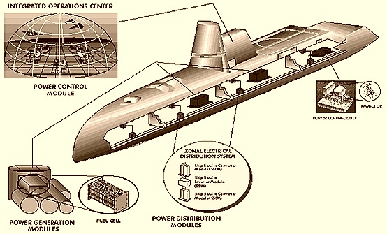

Conventional vs Electric Vehicle (EV)

Power Electronic Building Block (PEBB)-Based Power System
Physical Appearance of Few Power Electronic Devices
 POWER BJT
  POWER MOSFET
previous POWER ELECTRONICS (Introduction)
next Classification of Converters
POWER ELECTRONICS (Introduction)
Topics to be covered:
- What is Power Electronics?
- History of Power Electronics
- Application of Power Electronics
- Physical appearance of a few Power Electronic Devices
- Classification of Power Electronic Converters
- Design consideration of Power Electronic Equipment
- Role of transformers in Power Electronics
For descriptive purposes, it is frequently useful to divide the overall field of electrical engineering into three areas of specialization: electronics, power, and control. The electronics area deals primarily with devices and circuits for the processing of information; the power area deals with both rotating and static equipment for the generation, transmission, distribution, and utilization of vast quantities of electrical power; and the control area deals with the stability and response characteristics of closed-loop systems using feedback on either a continuous or sampled-data basis.
Interstitial to all three of these areas is power electronics, which deals with the use of electronics for the control and conversion of large amounts of electrical power.
“The task of power electronics (circuits/systems) is to process and control the flow of electric energy or power by supplying voltages and currents in a form that is optimally suited to the load.”
 Power Input:
- From electric utility: ac input, 1 or 3 phase, 50 or 60 Hz
- From dc supply/battery: dc input
- From previous converter output: ac/dc input
Power Converter Core : Using BJT/ MOSFET/ SCR/ GTO/ IGBT/ MCT as switch, Diode, L and C as energy manipulators
Power Output: to load (load can be of R or L or R-L nature) output parameters: dc/ac voltage, dc/ac current, frequency & number of phase

next Applications of Power Electronics
High-voltage electronics market and technology trends
The market for power electronics is booming in all voltage ranges!
More importantly, the power supply for applications markets> 1.7kV, such as wind turbines, transmission and distribution (T & D) railway traction and propulsion, and the ship complies with companies with high added value.
It is certain that your total market size 2010 405.000.000 $ (including power supplies and power modules) is expected to be small compared to markets with less tension but still very dynamic and offers the possibility of high margins.
This market is mainly motivated by considerations of energy conservation and the development of environmentally friendly technologies. They are supported - for example, T + D of electricity - from governments and large companies are working to improve its technology.
Since these IGBTs have thyristors (GTO and IGCT) and the diodes access to more and more technical improvements, such as the transition to 8 platforms oblea''y use of silicon carbide (SiC), among others.
But the long-term contracts for the production of small series and problems with raised blood components based on silicon carbide induce competition among the players fairly easily established markets.
Market parameters
Overall market for high-power devices and components (including IGBTs, thyristors and diodes) was 390 million € in 2009 and is expected to accelerate to more than $ 570,000,000 in 2015.
Traction to over 65% of this value for the high level of production that is driving the number of units per locomotive help.
T & D Power benefit from greater CAGR 2010-2015: 11.1%. In fact, we do expect a lot of work for the transport HDVC, and ABB offer a significant contribution to the architecture of HVDC Light IGBT.
Wind turbines have suffered from the crisis of 2009 and growth should be stronger the second from 2010 to 2015 CAGR of over 9%.
Finally, markets and ships were unevenly affected in 2009. Military ships continue to grow - a relatively long time of production of ships - all tourist yacht for private use is purchased declined dramatically. Accordingly, estimates IGBT module, the global market for ships and boats continue in 2013, reaching $ 26,000,000 in 2015.
Special Report
Power electronics are a daily challenge in many systems today (PV inverters, electric vehicles and hybrid electric, cameras, appliances, ...) from a market perspective, but also the development of technologies.
Many companies are growing R & D difficult to provide the most cost-effective, efficient and reliable materials, devices and systems. And the more "hidden" applications, such as benefit-1.7kV segment of the efforts described in this report.
The four segments were examined in this report:
- Converters for wind turbines
Power T & D -
- Rail Traction
- Ships and boats.
Due to the different scenarios, low interest in the development of marketing efforts and the level of the evolution of market revenue, automation and industrial UPS markets have described.
With a thorough knowledge of these markets Yole Development application provides a detailed analysis of each one:
- The technical developments leading
- The architecture of the inverter units
- Market data at a macro-level market: wind turbines installed base, ship and rail transportation and the number of existing electrical systems to T + D
- Market detection devices and energy modules, IGBTs, thyristors and diodes
- An estimate of the market for silicon wafers and silicon carbide penetration
- Thorough knowledge of the value chains
- Market shares of major companies
Voltage Source SPWM Inverter
During the positive cycle, S1 and S2 are switched by the high frequency pulse train shown in Figure (next slide). During the negative cycle, the pulse train switches S3 and S4. The load inductance integrates the generated pulse train and produces a sinusoidal voltage (Vac) and current wave, as shown in the next Figure. The width of each pulse is varied in proportion to the amplitude of a sine wave. A typical PWM waveform is shown in the previous slide. The switches in this converter are controlled by gate pulses. The gate signal contains several pulses distributed along the half-cycle. The control circuit produces the gate pulse train by generation of a triangular carrier wave and a sinusoidal reference signal. The two signals are compared, and when the carrier wave is larger than the reference signal, the gate signal is positive. When the carrier wave is smaller than the reference signal, the gate signal is zero. This results in a gate pulse with variable width.
 Figure: Single-phase voltage source converter.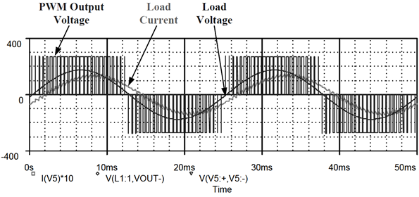
Figure: Gate pulse input signal, and ac voltage and current outputs of a pulse width modulation (PWM) converter.
 (a) Triangular carrier wave and sinusoidal reference signal
 (b) Variable-width gate pulse signal
Figure: Pulse width modulation (PWM) signals.
Figure (a) shows the carrier wave and reference sine wave; (b) depicts the resulting gate signal with variable width pulses. It has to be noted that several other methods are used for generation of PWM signals as discussed earlier.
The frequency of the reference sine wave determines the frequency of the generated ac voltage. The amplitude of the ac voltage can be regulated by the variation of the reference signal amplitude. The amplitude of the fundamental component of the ac voltage is:

The modulation index (m or M) is the ratio of the peak-to-peak ac voltage (2Vac) to the dc voltage.
Freewheeling diode
The inverter interrupts the current several times each cycle. The interruption of an inductive current would generate unacceptably high overvoltage. This over voltage generation is eliminated by providing freewheeling diodes connected in parallel with the switches.
previous Multiple-Pulse PWMnext Sinusoidal PWM
Basic Structure of IGBT
The basic schematic of a typical N-channel IGBT based upon the DMOS process is shown in Figure 1. This is one of several structures possible for this device. It is evident that the silicon cross-section of an IGBT is almost identical to that of a vertical Power MOSFET except for the P+ injecting layer. It shares similar MOS gate structure and P wells with N+ source regions. The N+ layer at the top is the source or emitter and the P+ layer at the bottom is the drain or collector. It is also feasible to make P-channel IGBTs and for which the doping profile in each layer will be reversed. IGBT has a parasitic thyristor comprising the four-layer NPNP structure. Turn-on of this thyristor is undesirable. Some IGBTs, manufactured without the N+ buffer layer, are called non punch through (NPT) IGBTs whereas those with this layer are called punch-through (PT) IGBTs. The presence of this buffer layer can significantly improve the performance of the device if the doping level and thickness of this layer are chosen appropriately. Despite physical similarities, the operation of an IGBT is closer to that of a power BJT than a power MOSFET. It is due to the P+ drain layer (injecting layer) which is responsible for the minority carrier injection into the N–drift region and the resulting conductivity modulation. Based on the structure, a simple equivalent circuit model of an IGBT can be drawn as shown in Figure 2.

Figure 1: Schematic view of a generic N-channel IGBT
It contains MOSFET, JFET, NPN and PNP transistors. The collector of the PNP is connected to the base of the NPN and the collector of the NPN is connected to the base of the PNP through the JFET. The NPN and PNP transistors represent the parasitic thyristor which constitutes a regenerative feedback loop. The resistor RB represents the shorting of the base-emitter of the NPN transistor to ensure that the thyristor does not latch up, which will lead to the IGBT latchup. The JFET represents the constriction of current between any two neighboring IGBT cells. It supports most of the voltage and allows the MOSFET to be a low voltage type and consequently have a low RDS(on) value. A circuit symbol for the IGBT is shown in Figure 3.

Figure 2: Equivalent circuit model of an IGBT

Figure 3: IGBT Circuit Symbol
Operation:Forward-Blocking and Conduction Modes:

When a positive voltage is applied across the collector-to-emitter terminal with gate shorted to emitter shown in Figure 1, the device enters into forward blocking mode with junctions J1 and J3 are forward-biased and junction J2 is reverse-biased. A depletion layer extends on both-sides of junction J2 partly into P-base and N-drift region. An IGBT in the forward-blocking state can be transferred to the forward conducting state by removing the gate-emitter shorting and applying a positive voltage of sufficient level to invert the Si below gate in the P base region. This forms a conducting channel which connects the N+ emitter to the N--drift region. Through this channel, electrons are transported from the N+ emitter to the N--drift. This flow of electrons into the N—drift lowers the potential of the N--drift region whereby the P+ collector/ N--drift becomes forward-biased. Under this forward-biased condition, a high density of minority carrier holes is injected into the N--drift from the P+ collector. When the injected carrier concentration is very much larger the background concentration, a condition defined as a plasma of holes builds up in the N--drift region. This plasma of holes attracts electrons from the emitter contact to maintain local charge neutrality. In this manner, approximately equal excess concentrations of holes and electrons are gathered in the N - drift region. This excess electron and hole concentrations drastically enhance the conductivity of N--drift region. This mechanism in rise in conductivity is referred to as the conductivity modulation of the N--drift region.
Reverse-Blocking Mode:
When a negative voltage is applied across the collector-to-emitter terminal shown in Figure 1, the junction J1 becomes reverse-biased and its depletion layer extends into the N--drift region. The break down voltage during the reverse-blocking is determined by an open-base BJT formed by the P+ collector/ N--drift/P-base regions. The device is prone to punch-through if the N--drift region is very lightly-doped. The desired reverse voltage capability can be obtained by optimizing the resistivity and thickness of the N—drift region.
The width of the N--drift region that determines the reverse voltage capability and the forward voltage drop which increases with increasing width can be determined by

LP = Minority carrier diffusion length
Vm = Maximum blocking voltage
?0 = Permittivity of free space
?s = Dielectric constant of Si
q = Electronic charge
ND = Doping concentration of N-drift region
Latch-up:

During on-state, paths for current flow in an IGBT are shown in Figure 10. The holes are injected into the N--drift region from the P+ collector form two paths. Part of the holes disappear by recombination with electrons came from MOSFET channel. Other part of holes are attracted to the vicinity of the inversion layer by the negative charge of electrons, travel laterally through the P-body layer and develops a voltage drop in the ohmic resistance of the body. This voltage tends to forward bias the N+P junction and if it is large enough, substantial injection of electrons from the emitter into the body region will occur and the parasiric NPN transistor will be turned-on. If this happens, both NPN and PNP parasitic transistors will be turned-on and hence the thyristor composed of these two transistors will latch on and the latchup condition of IGBT will have occurred. Once in latchup, the gate has no control on the collector current and the only way to turn-off the IGBT is by forced commutation of the current, exactly the same as for a conventional thyristor. If latchup is not terminated quickly, the IGBT will be destroyed by the excessive power dissipation. IGBT has a maximum allowable peak drain current (ICM) that can flow without latchup. Device manufacturers specify this current level in the datasheet. Beyond this current level, a large enough lateral voltage drop will activate thyristor and the latchup of IGBT.
Safe Operating Area (SOA)
The safe operating area (SOA) is defined as the current-voltage boundary within which a power switching device can be operated without destructive failure. For IGBT, the area is defined by the maximum collector-emitter voltage VCE and collector current IC within which the IGBT operation must be confined to protect it from damage. The IGBT has the following types of SOA operations: forward-biased safe operating area (FBSOA), reverse-biased safe operating area (RBSOA) and short-circuit safe operating area (SCSOA).
Three Phase Topology
| MODE | Sw1 | Sw2 | Sw3 | Sw4 | Sw5 | Sw6 | VAO | VBO | VCO |
| 1 | ON | OFF | OFF | OFF | ON | ON | +0.5 Edc | -0.5 Edc | +0.5 Edc |
| 2 | ON | ON | OFF | OFF | OFF | ON | +0.5 Edc | -0.5 Edc | -0.5 Edc |
| 3 | ON | ON | ON | OFF | OFF | OFF | +0.5 Edc | +0.5 Edc | -0.5 Edc |
| 4 | OFF | ON | ON | ON | OFF | OFF | -0.5 Edc | +0.5 Edc | -0.5 Edc |
| 5 | OFF | OFF | ON | ON | ON | OFF | -0.5 Edc | +0.5 Edc | +0.5 Edc |
| 6 | OFF | OFF | OFF | ON | ON | ON | -0.5 Edc | -0.5 Edc | +0.5 Edc |
| 7 | ON | OFF | OFF | OFF | ON | ON | +0.5 Edc | -0.5 Edc | +0.5 Edc |
| 8 | ON | ON | OFF | OFF | OFF | ON | +0.5 Edc | -0.5 Edc | -0.5 Edc |
| 9 | ON | ON | ON | OFF | OFF | OFF | +0.5 Edc | +0.5 Edc | -0.5 Edc |
| 10 | OFF | ON | ON | ON | OFF | OFF | -0.5 Edc | +0.5 Edc | -0.5 Edc |
| 11 | OFF | OFF | ON | ON | ON | OFF | -0.5 Edc | +0.5 Edc | +0.5 Edc |
| 12 | OFF | OFF | OFF | ON | ON | ON | -0.5 Edc | -0.5 Edc | +0.5 Edc |
VAB = VAO – VBO
VBC = VBO – VCO
VCA = VCO – VAO
Relationships between pole voltages (VAO, VBO, VCO) and phase voltages (VAN, VBN, VCN)
For a balance three phase system,
VAN + VBN + VCN = 0 (1)
and,
VAN = VAO – VNO (2.1)
VBN = VBO – VNO (2.2)
VCN = VCO – VNO (2.3)
(2.1), (2.2), and (2.3) into (1),
VAO + VBO + VCO – 3VNO = 0
Therefore VNO = 1/3(VAO + VBO + VCO)
(3) into (2.1),
VAN = VAO – 1/3(VAO + VBO + VCO) = 2/3 VAO - 1/3 (VBO + VCO)
(3) into (2.2),
VBN = 2/3 VBO – 1/3 (VAO + VCO)
(3) into (2.3),
VCN = 2/3 VCO – 1/3 (VAO + VBO)

Subscribe to:
Posts (Atom)


