previous INTRODUCTION TO MICROCONTROLLER PIC16F72 AND ACCESSOREIS
4.1 CALCULATIONS
4.1.1 ASSUMPTIONS
Let us assume that we have to generate a 50 Hz sine PWM. For this we need a triangular wave with 10 times the frequency of the desired sine wave. For simplicity we denote the factors with some symbols whose are listed below-
Vs = instantaneous voltage of the sine wave
Vm = maximum amplitude of the sine wave
f = frequency of the sine wave (50 Hz)
t = time
T = period of the sine wave (20 ms)
τ = half of the period (10 ms)
Vc = instantaneous voltage of the reference triangular wave
Vcm = maximum amplitude of the reference triangular wave
M = modulating index (0.8) =
4.1.2 EQUATIONS AND TIME CALCULATIONS
We have the equation of the sine wave is-
Vs = Vm sin ωt …………..(4.1)
For determining t1 according to figure 4.1 we get the equation for straight line containing t1 is-

And the equation for the sine wave remains-
Vs = Vm sin ωt1 …………(4.3)


Solving equation (4.5) we get the value of t1 -
t1 = 800.8429071 us
Similarly solving the equation considering the straight line containing t2 we get the value of t2-

Solving the equation considering the straight line containing t3 we get the value of t3 -

Solving the equation considering the straight line containing t4 we get the value of t4 -

Solving the equation considering the straight line containing t5 we get the value of t5 -
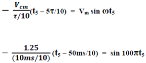
=> t5 = 4.223675159 ms
Solving the equation considering the straight line containing t6 we get the value of t6 -

Solving the equation considering the straight line containing t7 we get the value of t7 -

Solving the equation considering the straight line containing t8 we get the value of t8 -
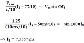
Solving the equation considering the straight line containing t9 we get the value of t9 -

Solving the equation considering the straight line containing t10 we get the value of t10 -

We have to accept some assumption on approximate values of these times because the microcontroller can not accept fractional values efficiently. Thus we get the following values of t –
t1 = 800.8429071 us ≈ 801us
t2 = 1.323 ms ≈ 1.323ms
t3 = 2.444299507 ms ≈ 2.444ms
t4 = 3.737938236 ms ≈ 3.738ms
t5 = 4.223675159 ms ≈ 4.224ms
t6 = 5.776324841 ms ≈ 5.776ms
t7 = 6.262061764 ms ≈ 6.262ms
t8 = 7.5557 ms ≈ 7.556ms
t9 = 8.676980416 ms ≈ 8.677ms
t10 = 9.199157093 ms ≈ 9.199ms
4.1.3 DURATIONS OF THE PULSES
From the ten intersection points with the times we get the durations of 5 high states and 6 low states for the first 1800 of the 1st phase. The approximate view is shown below-

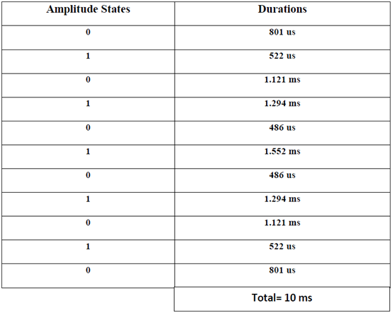
Here the durations are given according to time intervals with corresponding amplitude states-
Duration 1: (801us - 0 s) = 801 us
Duration 2: (1.323 ms - 801us) = 522 us
Duration 3: (2.444 ms - 1.323 ms) = 1.121 ms
Duration 4: (3.738 ms - 2.444 ms) = 1.294 ms
Duration 5: (4.224 ms - 3.738 ms) = 486 us
Duration 6: (5.776 ms - 4.224 ms) = 1.552 ms
Duration 7: (6.262 ms - 5.776 ms) = 486 us
Duration 8: (7.556 ms - 6.262 ms) = 1.294 ms
Duration 9: (8.677 ms - 7.556 ms) = 1.121 ms
Duration 10: (9.199 ms - 8.677 ms) = 522 us
Duration 11: (10 ms - 9.199 ms) = 801 us
The above data’s are arranged in the table 1 below-


4.2.1 DEFINING THE PORTS OF MICROCNTROLLER
Lets start from a simple programming in PIC16F72 using mikroC programming language.
void main()
{
trisa = 0b00000000; // defining all the pins of port A are output pins //
trisb = 0b00000000; // defining all the pins of port B are output pins //
while(1) // infinite loop creation //
{
portb=0b00000001; // changing the states of RB0, RB1 and RB2 to 1, 0 and 0 respectively //
porta=0b00000010; // changing the states of RA0, RA1 and RA2 to 0, 1 and 0 respectively //
delay_us(405); // holding the above states of the pins for 405 microsecond //
portb=0b00000001; // changing the states of RB0, RB1 and RB2 to 1, 0 and 0 respectively //
porta=0b00000000; // changing the states of RA0, RA1 and RA2 to 0, 0 and 0 respectively //
delay_us(396); // holding the above states of the pins for 396 microsecond // }
}
4.1 CALCULATIONS
4.1.1 ASSUMPTIONS
Let us assume that we have to generate a 50 Hz sine PWM. For this we need a triangular wave with 10 times the frequency of the desired sine wave. For simplicity we denote the factors with some symbols whose are listed below-
Vs = instantaneous voltage of the sine wave
Vm = maximum amplitude of the sine wave
f = frequency of the sine wave (50 Hz)
t = time
T = period of the sine wave (20 ms)
τ = half of the period (10 ms)
Vc = instantaneous voltage of the reference triangular wave
Vcm = maximum amplitude of the reference triangular wave
M = modulating index (0.8) =
4.1.2 EQUATIONS AND TIME CALCULATIONS
We have the equation of the sine wave is-
Vs = Vm sin ωt …………..(4.1)
For determining t1 according to figure 4.1 we get the equation for straight line containing t1 is-
And the equation for the sine wave remains-
Vs = Vm sin ωt1 …………(4.3)

Figure 4.1: Positive half comparison
For t1 we can equalize the two equations as below-
Solving equation (4.5) we get the value of t1 -
t1 = 800.8429071 us
Similarly solving the equation considering the straight line containing t2 we get the value of t2-

Solving the equation considering the straight line containing t3 we get the value of t3 -

Solving the equation considering the straight line containing t4 we get the value of t4 -

Solving the equation considering the straight line containing t5 we get the value of t5 -

=> t5 = 4.223675159 ms
Solving the equation considering the straight line containing t6 we get the value of t6 -

Solving the equation considering the straight line containing t7 we get the value of t7 -

Solving the equation considering the straight line containing t8 we get the value of t8 -

Solving the equation considering the straight line containing t9 we get the value of t9 -

Solving the equation considering the straight line containing t10 we get the value of t10 -

We have to accept some assumption on approximate values of these times because the microcontroller can not accept fractional values efficiently. Thus we get the following values of t –
t1 = 800.8429071 us ≈ 801us
t2 = 1.323 ms ≈ 1.323ms
t3 = 2.444299507 ms ≈ 2.444ms
t4 = 3.737938236 ms ≈ 3.738ms
t5 = 4.223675159 ms ≈ 4.224ms
t6 = 5.776324841 ms ≈ 5.776ms
t7 = 6.262061764 ms ≈ 6.262ms
t8 = 7.5557 ms ≈ 7.556ms
t9 = 8.676980416 ms ≈ 8.677ms
t10 = 9.199157093 ms ≈ 9.199ms
4.1.3 DURATIONS OF THE PULSES
From the ten intersection points with the times we get the durations of 5 high states and 6 low states for the first 1800 of the 1st phase. The approximate view is shown below-

Figure 4.2: First positive half cycle of the first phase
4.1.4 CALCULATIONS FOR THE DURATIONSHere the durations are given according to time intervals with corresponding amplitude states-
Duration 1: (801us - 0 s) = 801 us
Duration 2: (1.323 ms - 801us) = 522 us
Duration 3: (2.444 ms - 1.323 ms) = 1.121 ms
Duration 4: (3.738 ms - 2.444 ms) = 1.294 ms
Duration 5: (4.224 ms - 3.738 ms) = 486 us
Duration 6: (5.776 ms - 4.224 ms) = 1.552 ms
Duration 7: (6.262 ms - 5.776 ms) = 486 us
Duration 8: (7.556 ms - 6.262 ms) = 1.294 ms
Duration 9: (8.677 ms - 7.556 ms) = 1.121 ms
Duration 10: (9.199 ms - 8.677 ms) = 522 us
Duration 11: (10 ms - 9.199 ms) = 801 us
The above data’s are arranged in the table 1 below-
Table 1: Logic states of PWM
4.1.5 THREE PHASE ASSUMPTIONS AND LOGIC STATES
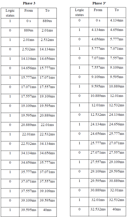
Now for the other phases and their logic states we have to calculate the phase shift of the subsequent phases in terms of delay in ms or us. As it is very lengthy process to show the calculation we only show the logic states and their corresponding duration or time ranges. These are shown in the following figure and then the calculated values are shown in tables-
Figure 4.3: Three phase representation in terms of six gate signals


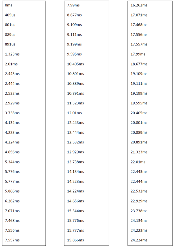
From the above tables taking the times from 0 second to 40 ms sequentially we get the following Set of times-
As the above data’s are in huge number they can not be plotted in a single figure. Setting only the times in figure 4.4 and figure 4.5 we get six logic states for every time intervals listed above.
Figure 4.4: 1st half logical states of six phase pulses
Figure 4.5: 2nd logical states of six phase pulses
4.2 PWM IMPLEMENTATION4.2.1 DEFINING THE PORTS OF MICROCNTROLLER
In the figures the phase sequence is phase 1, phase 2, phase 3, phase 1', phase 2', phase 3'.from the figures 4.4 & 4.5 we can now arrange the programming process in the microcontroller. For final touch we arrange the phase according to pin of the microcontroller. We have use the first 3 pins of port B for Phase 1, Phase 2 and Phase 3 respectively and first 3 pins of port A for Phase 1', Phase 2' and Phase 3' respectively. The pin logical states are shown below where first 3 states for port B ( RB0, RB1 and RB2 respectively ) and the next 3 states for port A ( RA0, RA1 and RA2 respectively ) . The durations are calculated subtracting two consecutive instant of time with the corresponding logical states (as shown in figure 4.4 and figure 4.5).
4.2.2 PROGRAMMING THE MICROCONTROLLERLets start from a simple programming in PIC16F72 using mikroC programming language.
void main()
{
trisa = 0b00000000; // defining all the pins of port A are output pins //
trisb = 0b00000000; // defining all the pins of port B are output pins //
while(1) // infinite loop creation //
{
portb=0b00000001; // changing the states of RB0, RB1 and RB2 to 1, 0 and 0 respectively //
porta=0b00000010; // changing the states of RA0, RA1 and RA2 to 0, 1 and 0 respectively //
delay_us(405); // holding the above states of the pins for 405 microsecond //
portb=0b00000001; // changing the states of RB0, RB1 and RB2 to 1, 0 and 0 respectively //
porta=0b00000000; // changing the states of RA0, RA1 and RA2 to 0, 0 and 0 respectively //
delay_us(396); // holding the above states of the pins for 396 microsecond // }
}
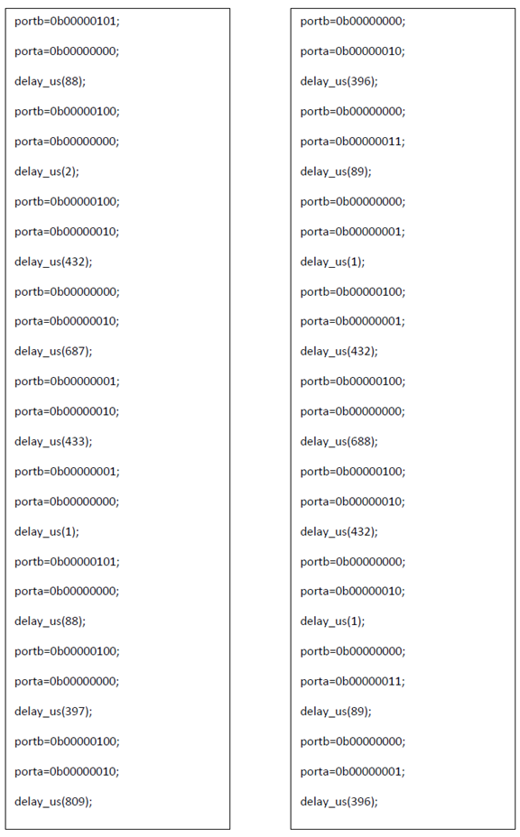
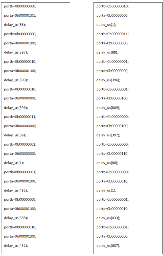
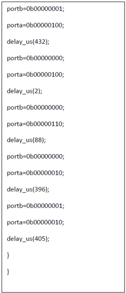
The above change of states will be repeated infinitely. Now we can implement similarly our desired program using the format shown above. The program is given below-
4.2.3 CIRCUIT DIAGRAM
From the datasheet of PIC16F72 we know that port B consist of 8 pins starting from pin 21 to pin 28 denoting RB0, RB1, RB2, RB3, RB4, RB5, RB6 and RB7 and port A consist of 6 pins starting from pin 2 to pin 7. Also have a reset pin that should be connected to Vdd. According to the program the connection diagram is shown in figure 4.6. We have the phases denoted by Phase 1 from pin no. 21 (RB0), phase 2 from pin no. 22 (RB1), phase 3 from pin no. 23 (RB2), phase 1' from pin no. 2 (RA0), phase 2' from pin no. 3 (RA1) and phase 3' from pin no. 4 (RA2). The connection in Breadboard with the resultant wave forms we get from oscilloscope are shown below subsequently.
Figure 4.6: Connection diagram of PIC16F72 for six phase SPWM
4.3 OVERALL BLOCK DIAGRAM OF THE PROCEDURE
The step by step process is very lengthy. So for easy understanding the overall process, calculation and implementation process is explained in the following block diagram-






No comments:
Post a Comment
Please wait for approval of your comment .......