Presentation on DESIGN & IMPLEMENTATION OF BOOST INVERTER AN INTERFACE BETWEEN PHOTOVOLTAIC SYSTEM AND POWER UTILITIES
INTRODUCTION
- The global electrical energy consumption is steadily rising.
- Therefore a continuous demand to increase the power generation capacity.
- Photovoltaic system is one of the cost effective renewable energy conversion system.
OBJECTIVES
- An interfacing device dc-ac boost inverter have been used between photovoltaic system and power utilities.
- To invert 12V dc input of photovoltaic cell to 220V ac (50Hz).
- To reduce energy losses and harmonics P. W. M. voltage source inverter strategy is used.
- An interfacing device dc-ac boost inverter have been used between photovoltaic system and power utilities.
- To invert 12V dc input of photovoltaic cell to 220V ac (50Hz).
- To reduce energy losses and harmonics P. W. M. voltage source inverter strategy is used.
EXPLANATION
A traditional design methodology is the use of buck inverter. One of the characteristics of the most classical inverter is that it produces an ac output instantaneous voltage always lower then the dc input voltage. Thus if an output voltage higher then the input one is needed, a boost dc-dc must be used between the dc source and the inverter. The full bridge topology can however be used as a boost inverter that can greater an output ac voltage that the input dc voltage.
Fig: Conversion of solar cell to home application
BOOST REGULATORBoost Converter is a power converter whose output voltage is greater than input voltage.
The output level of a boost converter is controlled by the duty cycle of a switching pulse.
The input output relationship is-
Vo =Vin/(1-D).PRINCIPLE OF BOOST INVERTER
When two dc-dc converters feeding a resistive load, then they produce a dc biased sine wave output, such a way each source only produces a unipolar voltage. The modulation of each converter is 180o out of phase with the other so the voltage excursion across the load is maximized.
A dc biased voltage appears at each end of the load with respect to the ground. But the differential dc voltage across the load is zero, only ac voltage appears.
ADVANTAGES OF BOOST INVERTER- Step up the output voltage without a transformer.
- High efficiency.
- Continuous input current.
Fig.1: Unipolar voltage across both converter 180 o phase shift
Fig.2: Differential voltage across load
PWM STRATEGY
If dc input voltage is fixed, a variable output voltage can be obtained by varying the gain of the inverter, which is normally accomplished by Pulse-Width-Modulation (PWM) control within the inverter.
Switching techniques minimizes the harmonic contents of output voltage and low distorted sinusoidal waveforms are obtained.
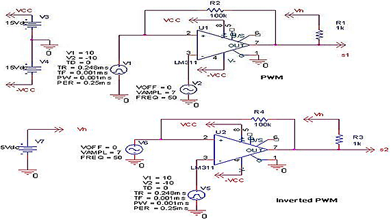
Switching or control circuit
PWM & INVERTED PWM
LOCK OUT CIRCUIT
Theoretically we consider the pulses have no rise time and fall time, but practically they have. When two pulses used those are identical but invert of one another in current bidirectional boost converter where two IGBT are connected serially may cause problems. At the time when the pulses are rising or falling both of the two IGBTs are on and there will create a short path, so a large current flows through them which can burn the IGBT.
The problem is overcome by a circuit, lock out circuit. The basic is, at the time of rising or falling, it is forced to be zero at the switching end. So that the transition period is overcome.
LOCK OUT WAVEFORM
GROUND ISOLATION
There are many situations where signals and data need to be transferred from one subsystem to another within a piece of electronics equipment, or from one piece of equipment to another, without making a direct ohmic electrical connection. Often this is because the source and destination are (or may be at times) at very different voltage levels. Like a lock out circuit, consists of logic gates which is operating from 5V DC but being used to control a IGBT which is switching 240V AC. In such situations the link between the two must be an isolated one, to protect the switching circuit / IGBT from overvoltage damage.
THD FOR DIFFERENT LOAD CONDITION
| Resistive loads (ohm) | THD % |
| 50 | 4.13 |
| 100 | 3.60 |
| 150 | 3.46 |
| 200 | 3.40 |
| 250 | 3.47 |
| 500 | 3.52 |
| 1k | 3.57 |
| Inductive load (mH) with Resistive load(200 ohm) | THD% |
| 5 | 3.45 |
| 10 | 3.44 |
| 20 | 3.43 |
| 25 | 3.42 |
| 50 | 3.47 |
| 75 | 3.50 |
| 100 | 3.53 |
CURRENT AND VOLTAGE AT LOAD with 200ohm and 5 mH load with input 12Vdc
SUMMERY OF RESULT- THD of output voltage maintain the IEEE standard, which is for 0 ~ 240V THD ≤ 5%.
- Optimum THD is 3.40% for resistive load 200 ohm.
- For inductive load 25 mH THD 3.42% is optimum.
COMPLETE SETUP
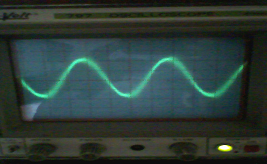
OUTPUT WAVEFORM OF INVERSION CIRCUIT WITH LOAD 200 OHMS
FUTURE WORK- Output voltage stabilization.
- Multilevel output. (Single phase 120V at 60Hz, 220V at 50Hz, 115V at 400Hz)
In this project we tried to implement a new type dc to ac inverter. We use IGBTs as active switches which operate at fixed frequency. Here we use different linear and non linear loads. Our experimental result is not completely coping with the proposed theory. Because in our simulation we used the ideal conception, practically our equipments are not ideal at all. If we avert this problem we will reach to our desired goal. The new inverter is applicable in solar home application and UPS design when the ac voltage is larger than the dc link voltage is needed, with no need of second power conversion stages.
Submitted by OVIJIT KURI and SK. MD. GOLAM MOSTAFA


Hi, thanks for the information on boost inverter interface, this helped me a lot in choosing the best On line ups Dealers in Chennai
ReplyDeleteI'm trying to understand this design. Observing the boost inverter circuit the top left IGBT gate is being switched by s5 and the bottom right is switched by s8. Where is s5 and s8 in the design? also why is s6 being used on the emitter of the top left igbt
ReplyDeleteThe pspice circuit doesn't work.
ReplyDelete