IGBT is turned on by applying a positive voltage between the gate and emitter and is turned off by making the gate signal zero or slightly negative.
IGBT has low on-state voltage drop and high off-state voltage characteristics with the excellent switching characteristics, simple gate-drive circuit, peak current capability and high input impedance.
IGBTs are available in current and voltage ratings well beyond what is normally available for power MOSFETs.
IGBTs are replacing power MOSFETs in high-voltage applications where conduction losses must be kept low. The IGBT has a much lower voltage drop than a MOSFET of similar ratings.
The switching speed of an IGBT is faster than a BJT but inferior to that of MOSFETs.
IGBTs do not have second breakdown problem due to its physical structure is similar to that of power MOSFETs. SOA is similar to that OSFET.
")
Characteristics of IGBT
The i-v characteristics appears qualitatively similar to that of a logic level BJT except that the controlling parameter is an input voltage.
The transfer curve ic-vGE is identical to that of the power MOSFET except VGE(th) and the slope values.
Structure of IGBT
In general, IGBTs can be classified as punch-through (PT) and nonpunch-through (NPT) structures. Fig. below shows the PT structure here and n+ buffer layer is normally introduced between the p+ substrate and the n- -epitaxial layer, so that the whole n- drift region is depleted when the device is blocking the off-state voltage, and the electrical field shape inside the n- drift region is close to a rectangular shape. Because a shorter n- region can be used in the punch-through IGBT, a better trade-off between the forward voltage drop and turn-off time can be achieved. PT IGBTs are available up to about 1200 V.
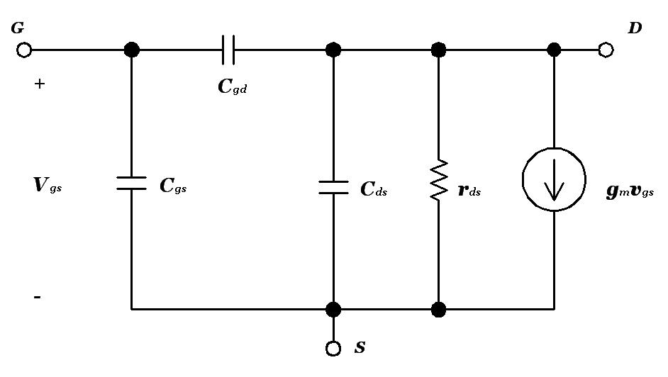
Circuit Model of IGBT and Operating Principle
Operation is similar to that of MOSFET except the resistance offered by the top n region, which is very much similar during on-state.
The decrease in resistance occurs because of the injection of holes from the top p+ zone into the n zone. This effect is called conductivity modulation of the n region.
RRR- body region spreading resistance.
RMOD- modulated resistance due to carrier injection from the top p+ zone.
Channel (drain) current of MOSFET is the base current of pnp transistor.
Collector current of pnp transistor is the base current of npn transistor.
Operating Principle of IGBT
If C is positive with respect to E and if G is positive with respect to E greater than the threshold level, n channel is created, current flows through the channel (D to S) of the MOSFET.
The current flowing through the channel serves as the base current for pnp transistor, which causes emitter current to flow in this transistor resulting in the large-scale injection of holes across the top pn junction-these holes are responsible for the conductivity modulation of the middle n zone.
Saturation voltage characteristics of IGBT
Ron of an IGBT is usually 10 times smaller than that of a power MOSFET of the same size and voltage capability. This is because of the conductivity modulation process in the drift region.
The major current flow through the drive MOSFET again because of the conductivity modulation of the drift region.
VCE(sat) = VJ1 + Vdrift + IDRchannel
Where VJ1 ~ 0.7 – 1.0 V,
Vdrift < that of power MOSFET, and IDRchannel ~ that of power MOSFET
Normally, the on-state or saturation voltage drop is used is instead of on-state resistance.
Even in IGBTs with the same structure, the IGBT with a fast switching speed has a larger on-state voltage drop, and vice-versa.
The on-state voltage changes little between room temperature and the maximum junction temperature. This is because of the combination of positive temperature coefficient of the MOSFET section and the negative temperature coefficient of the voltage drop across the drift region.
Safe Operating area (SOA) of IGBT
The FBSOA defines a maximum V-I region in which the device can be commanded to operate with simultaneous high voltage and current. The device current can be controlled through its gate (or base) and the length of the operation is only limited by its thermal limitation. Device with FBSOA normally have an active region in which the device current is determined by the control signal level. Example IGBT….
Forward Biased Safe operating Area (SOA) of IGBT
SOAs
-
The FBSOA is identical to that of the power MOSFET.
-
The RBSOA (for turn-off) is different from the FBSOA. The reapplied dvCE/dt is limited to avoid the latch-up of IGBT (or latch-on of the parasitic thyristor). But the values are quit large which can be easily controlled by the gate. If latch-up occurs, it must be terminated quickly, otherwise the IGBT will be destroyed.
-
The allowable maximum temperature, TJ(max) is 150°C.
-
The maximum collector current can be 4 to 10 times the normal rated current for 5-10µs depending on the value of VCE.
Commercial individual IGBTs and IGBT modules
-
Commercial individual available IGBTs have nominal current ratings as large as 200-400 A and voltage ratings as 1700V. voltage rating up to 2-3kV are projected. (The voltage ratings of IGBTs are higher than those of BJTs due to the small current gain of the pnp BJT.)
-
For a 1kV device, the on-state voltage is 2-3 V at rated current.
-
The turn-on and turned-off times are less than 1µs.
-
IGBTs are available in module in which 4 to 6 individual IGBTs are connected in parallel. Hence, the current ratings are in the ranged of 1000 to 1500 A.
Typical Gate drive Circuit for IGBT modules
IGBT Characteristics: a comparison
The IGBT characteristics in comparison with BJT, MOSFET with similar size and ratings.
Features
|
BJT
|
MOSFET
|
IGBT
|
Drive method
|
Current
|
Voltage
|
Voltage
|
Drive circuit
|
Complex
|
Simple
|
Simple
|
Input impedance
|
Low
|
High
|
High
|
Drive power
|
High
|
Low
|
Low
|
Switching speed
|
Slow (µs)
|
Fast (ns)
|
Medium
|
Operating frequency
|
Low (< 100 kHz)
|
Fast (<1 MHz)
|
Medium
|
SOA
|
Narrow
|
Wide
|
Wide
|
Saturation voltage
|
Low
|
High
|
Low
|
previous Power MOSFETs
next MOS controlled Thyristors (MCTs)


")