Power Semiconductor Devices

More on this category »

Latest Post

Familiarization with the IGBT Chopper/Inverter module

DISCUSSION
Description of the module
The IGBT Chopper / Inverter module mainly consists of 7 insulated-gate bipolar transistors (IGBT). An IGBT is a switching transistor that requires voltage on the gate to conduct. The IGBTs of the IGBT Chopper/Inverter module are labeled Q1 to Q7. IGBTs Q1 to Q6 are grouped in pairs as follows: Q1 with Q4, Q2 with Q5 and Q3 with Q6 and Q7 is part of the breaking circuit which limits the voltage on the DC bus. The module also contains electronic circuitry that isolates the gate of IGBTs and protects the IGBTs against overheating, overvoltage and over current.
F7-6 shows the front panel of the IGBT Chopper / Inverter Module. It shows many important characteristics about the operation of the module.
The DC voltage is applied through terminals 1 and 2 to supply the DC bus.
The DC bus is linked to IGBT Q1 and Q4 to supply loads from terminal 3. The DC bus may also be linked to IGBTs Q2 and Q5 through switch S1 and to IGBTs Q3 and Q6 through switch S2 to supply three- phase loads from terminals 3, 4 and 5.
Capacitor C1 is used to maintain a smooth DC voltage in spite of the current pulsations produced by the IGBTs. It is connected between terminals 1 and 2.
A power diode is connected between the collector and emitter of each IGBT. The diodes connected in parallel with the IGBTs have a very short recovery time. This important feature allows the IGBT Chopper / Inverter module to be used in high speed power switching circuits.
Front panel of the IGBT Chopper / Inverter module
F7-6: Front panel of the IGBT Chopper / Inverter module.
Protection circuits
The IGBT Chopper / Inverter module contains many electronic circuits that protect the IGBTs against various types of overloads. The operation of each protection circuit is briefly described in the following paragraphs.
The positive and negative branches of the DC bus are individually protected by breakers. When an overload condition occurs on the DC bus, one of the breakers trips. Correct the faulty condition and corresponding pushbutton to reset the breaker.
Over current protection circuit
The over current protection circuit is designed to protect IGBTs Q1 to Q6 against instantaneous over current. When an over current condition is detected on either IGBT, the six IGBTs are switched off by setting the gate voltage at 0 V. when this condition occurs, the OVERCURRENT LED turns on. The OVERCURRENT RESET pushbutton must be depressed to reset this protection circuit.
Overvoltage protection circuit
The overvoltage protection circuit is designed to protect IGBTs Q1 to Q6. This protection circuit senses the DC bus voltage. When the voltage exceeds a safe value, the six IGBTs are switched off by setting the gate voltage at 0 V and the OVERVOLTAGE LED turns on t indicate the faulty condition. The overvoltage protection circuit is automatically deactivated when the DC bus voltage returns to a safe value.
Overheat protection circuit
IGBTs Q1 to Q6 are also protected against overheating. The overheat protection circuit senses the heat sink temperature of the IGBTs. When the temperature exceeds a safe value, the six IGBTs are switched off by setting the gate voltage at 0 V and the OVERHEAT LED turns on to indicate the faulty condition. The overheating protection circuit is automatically deactivated when the temperature returns to safe value.
Breaking circuit
The breaking circuit consists mainly of the diode D7, resistor R1 and IGBT Q7 shown on the module panel. This circuit is designed to dissipate the energy produced by a decelerating motor connected to the IGBT Chopper / Inverter module. When the motor decelerates, it behaves like a generator and some power is returned to the DC bus. When the DC bus voltage exceeds a safe level, the braking circuit transfers some energy from the DC bus to resistor R1 and the BRAKING LED flashes. Notice that the module continues to operate in this condition. The braking circuit may be disabled by setting the BRAKING switch at 0.
Interconnection with control module
The gate of IGBTs Q1 to Q6 is connected to the SWITCHING CONTROL INPUTS connector through a series of internal isolators and amplifiers. This 9-pin connector may be connected to the CONTROL OUTPUTS of the Chopper/Inverter Control Unit module, or to the FIRING CONTROL OUTPUTS of the Thyristro Firing Unit.  
The pin configuration of the SWITCHING CONTROL INPUTS connector is given in F7-6. The inputs (pins 1 to 6) require 0-5 V transition of the control signals. Pin 7 is used to input a synchronization signal coming from the Chopper/Inverter Control Unit or the Thyristor Firing Unit.
The miniature banana jacks identified SWITCHING CONTROL INPUTS 1 to 6 are parallel connected to pins 1 to 6 of the SWITCHING CONTROL INPUTS 9-pin connector, respectively. This allows switching control signals coming from other equipment to be used to control the IGBTs.
The SYNC. OUTPUT miniature banana jack provides the synchronization signal coming from the Chopper/Inverter Control Unit or from the Thyristor Firing Unit. This 0-5 V signal may be used to synchronize an oscilloscope when observing the switching control signals.
The SWITCHING CONTROL INPUTS  DISABLE miniature banana jack allows to switch off IGBTs Q1 to Q6 by applying a +5-V voltage to this jack. In this condition, the IGBT gate voltage is 0 V, and the IGBTs cannot be controlled. They can be controlled when the SWITCHING CONTROL INPUTS DISABLE miniature banana jack is simply left open or connected to the common.
A 24-V AC power supply must be connected to either one of the two LOW POWER INPUT jacks to supply the electronic circuits. The POWER ON LED lights when AC voltage is applied.
The chassis terminal (green) on the front panel of the IGBT Chopper / Inverter module is used to prevent harmful electromagnetic emissions from interfering with other components. To do so, the shield of a special connection cable must be connected to this terminal.
Using the IGBT Chopper / Inverter module
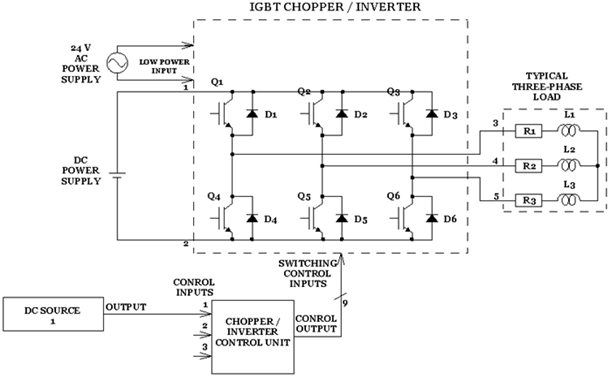
The IGBT Chopper / Inverter module is used to build various power electronic circuits such as choppers and inverters. F7-7 and 7-8 show examples of such power electronics circuits.
In the circuit of F7-7, IGBT Q1 and power diode D4 are used to build a bulk chopper. IGBT Q4 (parallel connected to power diode D4) and power diode D1 (parallel connected to IGBT Q1) are not shown in the figure because they are not used in this circuit.
In this circuit, SWITCHING CONTROL INPUT 4 of the IGBT Chopper / Inverter module is connected to common point to prevent IGBT Q4 from being switched on.
Buck chopper built using the IGBT Chopper / Inverter module
F7-7: Buck chopper built using the IGBT Chopper / Inverter module.
In the circuit of F7-8, the six IGBT Chopper / Inverter module form a three-phase inverter.
In the circuit of F7-7 and 7-8, the Chopper/Inverter Control Unit provides the control signals required to switch the IGBTs on or off.
Notice that in both circuits, a 24-V AC power supply is connected to the LOW POWER INPUT of the IGBT Chopper / Inverter module to supply the internal circuits. Also, notice that the capacitor connected on the DC bus has been intentionally omitted to simplify the diagrams.
The IGBT Chopper / Inverter module can be used with the Thyristor Firing Unit to build the Three-phase inverter shown in F7-8.

Three-phase inverter built using the IGBT Chopper / Inverter module
F7-8: Three-phase inverter built using the IGBT Chopper / Inverter module.

Familiarization with the Chopper/Inverter Control Unit (Inverter Modes)

OBJECTIVE
To learn how to use the Chopper/Inverter Control Unit in the various inverter modes.
DISCUSSION
Introduction
The Chopper/Inverter Control Unit is a control element which is especially designed to build two major types of power electronic circuits: choppers and inverters.
There are ten modes in which the Chopper/Inverter Control Unit can operate. These modes are listed below.
OFF- Standby
CHOP. PWM- Pulse-width modulation (PWM) control chopper
CHOP. STEPS- Two-step control chopper
3~ 120˚- 120˚-modulation three-phase inverter
3~ 180˚- 180˚-modulation three-phase inverter
3~ P1- Programmed-waveform 1 modulation three-phase inverter
3~ P2- Programmed-waveform 2 modulation three-phase inverter
3~ V/f- Constant V/f ratio three-phase inverter
2~ 180˚- 180˚-modulation two-phase inverter
AUX.- Auxiliary
In the OFF mode, the Chopper/Inverter Control Unit runs in a standby condition where it generates no control signals. Notice that the Chopper/Inverter Control Unit also runs in the standby condition in the AUX. mode. This mode is kept available for future developments.
The Pulse Width Modulation (CHOP. PWM), and two-step control (CHOP. STEPS) modes of the Chopper/Inverter Control Unit are used to build various types of choppers.
The other modes of the Chopper/Inverter Control Unit, that is 3--120˚, 3--180˚, 3—P1, 3—p2, 3—V/f and 2--180˚ are used to build various types of choppers. These modes have dealt with in section.
The 180˚-modulation three-phase inverter MODE (3- 180˚)
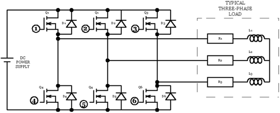
In this mode, the Chopper/Inverter Control Unit generates pulse signals designed to control a three-phase inverter. F6-1 shows the schematic diagram of a three-phase inverter built with power MOSFETs. Notice that the gate of each MOSFET is left open in this figure. Each gate only needs to be connected, through an isolator and an amplifier, to an appropriate control circuit, such as the Chopper/Inverter Control Unit, to complete the schematic diagram of the three-phase inverter.
Schematic diagram of a three-phase inverter built with power MOSFETS
F 6-1: Schematic diagram of a three-phase inverter built with power MOSFETS.
F6-2 shows an example of the control signals which the Chopper/Inverter Control Unit generates in the 3- 180˚ MODE. These signals, numbered 1 to 6, can be injected through isolators and amplifier into the MOSFET gates bearing the same number in the schematic diagram of the three-phase inverter shown in F6-1. Notice that control signals 1 to 6 are available on pins 1 t0 6 of the CONTROL OUTPUTS connector, respectively. In brief, the control signals switch the MOSFETs on and off in sequence to deliver ac power to the load. Since the duty cycle of the control signals is equal to 0.5, each MOSFET in the three-phase inverter shown in F6-1 is on 50% of time. In such a case, the inverter is referred to a 180˚-modulation three-phase inverter.
Control signals generated by the Chopper/Inverter Control Unit in the 3-180˚ MODE (positive voltage applied to Control INPUT 1)
F6-2: Control signals generated by the Chopper/Inverter Control Unit in the 3-180˚ MODE (positive voltage applied to Control INPUT 1).
The control signal frequency and the phase sequence of the control signals can be varied using CONTROL INPUT 1. The frequency varies linearly from 0 t 127 Hz as the voltage applied to CONTROL INPUT 1 varies from 0 to +10 V. in this case; the phase sequence of the control signals is as shown in F6-2. The control signal frequency varies again linearly from 0 to 127 Hz as the voltage applied to CONTROL INPUT 1 varies from 0 to +10 V, but this time the phase sequence of the control signals is reversed, as shown in F6-3. This feature is very useful when a three-phase inverter is used to control the speed of a motor which can rotate in both directions. CONTROL INPUTS 2 and 3 are not used in the 3~ 180˚ MODE.
Control signal generated by the Chopper/Inverter Control Unit in the 3~ 180˚ MODE (negative voltage applied to CONTROL INPUT 1)
F6-3: Control signal generated by the Chopper/Inverter Control Unit in the 3~ 180˚ MODE (negative voltage applied to CONTROL INPUT 1).
The 120˚-modulation, programmed waveform 1, and programmed waveform 2 three-phase inverter MODEs (3~ 120˚, 3~ P1 and 3~ P2)

In these modes the Chopper/Inverter Control Unit generates other types of pulse signals designed to control a three-phase inverter.

F6-4 shows an example of the control signals which the Chopper/Inverter Control Unit generates in the 3~ 120˚ MODE. These signals are identical to those generated in the 3~ 180˚ MODE (shown in F6-2) except that their duty cycle is equal to 0.33 instead of 0.5. An inverter with such control signals is referred to as a 120˚-modulation three-phase inverter.
Control signals generated by the Chopper/Inverter Control Unit in the 3~ 120˚ MODE (positive voltage applied to CONTROL INPUT 1)
F6-4: Control signals generated by the Chopper/Inverter Control Unit in the 3~ 120˚ MODE (positive voltage applied to CONTROL INPUT 1).
F6-5 and 6-6 show examples of the control signals which the Copper/Inverter Control Unit generates in the 3~ P1 MODEs, respectively. These signals consist of pulse trains which approximate the waveforms of the signals which are generated in the 3~ 180˚ MODE. The purpose of using a pulse train to approximate a waveform is to limit harmonic generation, which otherwise, could cause problems in many power electronics circuits.
Control signals generated by the Chopper/Inverter Control Unit in the   3~ P1 Mode (positive voltage applied to CONTROL INPUT 1)
F6-5: Control signals generated by the Chopper/Inverter Control Unit in the   3~ P1 Mode (positive voltage applied to CONTROL INPUT 1).
In these three modes, CONTROL INPUT 1 has the same function as in the 3~ 180˚ MODE, that is, the voltage applied to this input sets the control signal frequency and the phase sequence of the control signals. CONTROL INPUTS 2 and 3 are not used in any of these three modes.

Familiarization with the Chopper/Inverter Control Unit (Chopper Modes)

OBJECTIVE

To learn how to use the Chopper/Inverter Control Unit in the various chopper modes.

DISCUSSION

Introduction

The Chopper/Inverter Control Unit, whose front panel is shown in F5-1, is a control element which is especially designed to build two major types of power electronic circuits: choppers and inverters.

There are ten modes in which the Chopper/Inverter Control Unit can operate. These modes are listed below.

OFF-Standby

CHOP. PWM-Pulse-width modulation (PWM) control chopper

CHOP. STEPS-Two-step control chopper

3- 120˚-120˚-modulation three-phase inverter

3- 180˚-180˚-modulation three-phase inverter

3-P1-Programmed-waveform 1 modulation three-phase inverter

3-P2-Programmed-waveform 2 modulation three-phase inverter

3-V/f-Constant V/f ratio three-phase inverter

2-180˚-180˚ -modulation two-phase inverter

AUX.-Auxiliary

In the OFF mode, the Chopper/Inverter Control Unit runs in a standby condition where it generates no control signals. Notice that the Chopper/Inverter Control Unit also runs in the standby condition in the AUX. mode. This mode is kept available for future developments.

The Pulse-Width Modulation (CHOP. PWM) and two-step control (CHOP.STEPS) modes of the Chopper/Inverter Control Unit are used to build various types of choppers. These modes are dealt with in this section.

Six other modes of the Chopper/Inverter Control Unit, that is 3--120˚, 3--180˚, 3—P1, 3—P2, 3—V/f and 1--180˚, are used to build various types of choppers.

The front panel of the Chopper/Inverter Control Unit is divided into five sections which are described in the following subsections.

Front panel of the Chopper/Inverter Control Unit

F5-1: Front panel of the Chopper/Inverter Control Unit.

The MODE section

This section allows the mode in which the Chopper/Inverter Control Unit operates to be selected. The OFF MODE is automatically selected when the module is powered up. Successive modes in the list shown on the front panel of the module are selected when the SELECT. push button is brifly depressed. The selected mode enters into operation only after a delay of approximately 2 seconds. A LED in the MODE display light up to idicate the selected mode. Notice that the OFF MODE is selected when the SELECT. push button is depressed during more than approximately 0.5 second.

The CONTROL INPUTS section

This section consists of three inputs which can receive signals whose voltage can vary from -10 to +10 V. these inputs are numbered 1, 2 and 3. The function assigned to each input depends on the mode in which the Chopper/Inverter Control Unit operates. The function assigned to each input, depending on the operating mode of the Chopper/Inverter Control Unit, is described further in this discussion.

The CONTROL OUTPUT section

The 9-pin connector of this section provides control signals (pulse signals) which are used to switch power transistors on or off, such as those in the MOSFET Chopper / Inverter module. These control signals can also be used to trigger power devices such as the thyristors in the Power Thyristor module.

The pin configuration of the CONTROL OUTPUTS connector is same as shown in F2-3. Pins 1 to 6 provide 0-5 V level signals for controlling power devices Q1 to Q6 of power modules such as the MOSFET Chopper / Inverter or the Power Thyristors. Pin 7 provides a synchronization signal which is useful to synchronize the oscilloscope when observing the control signals. Pins 8 and 9 are connected to the common point of the Chopper/Inverter Control Unit.

The DC SOURCE 1 and DC SOURCE 2 section

Each of these sections provides a dc voltage which can be set between -10 and +10 V. Each of these voltages can be injected into one of the CONTROL INPUTS of the module, where it controls a given parameter. The nature of this parameter depends on the mode in which the Chopper/Inverter Control Unit operates. The OUTPUT voltage is -10 V when the control knob is set to min. position. The OUTPUT voltage is +10 V when the control knob is set to MAX. position.

The PWM-control chopper MODE (CHOP. PWM)

In this mode, the Chopper/Inverter Control Unit generates pulse-width modulation (PWM) signals designed to control a chopper. In this case, the chopper is pften referred to as a PWM-control chopper. F5-2 shows the schematic diagrams of various types of choppers built with power MOSFETs. Notice that the gate of each MOSFET is left open in this figure. Each gate only needs to be connected, through an isolator and an amplifier, to an appropriate control circuit, such as the Chopper/Inverter Control Unit, to complete the schematic diagram of each chopper.

A BUCK CHOPPER

a)     A BUCK CHOPPER

A BOOST CHOPPER

b)     A BOOST CHOPPER

A BUCK/BOOST CHOPPER  

c)     A BUCK/BOOST CHOPPER

   A FOUR-QUADRANT CHOPPER

d)     A FOUR-QUADRANT CHOPPER

F5-2: Schematic diagrams of various types of choppers built with power MOSFETs.

F5-2 shows an example of the PWM control signals which the Chopper/Inverter Control Unit generates in the CHOP. PWM MODE. These signals, which are numbered 1, 2, 4 and 5, can be injected, through isolators and amplifiers, into the MOSFET gates bearing the same number in the schematic diagrams of choppers shown in F5-2. In brief, one or many of these signals are used, according to the type of chopper, to switch the MOSFET on and off and deliver a certain amount of power to the load. Varying the duty cycle of the PWM control signals allows the amount of power delivered to the load to be varied. The duty cycle is defined as the ratio of the pulse duration to the duration of one cycle of the pulse signal. Note that PWM control signals 1, 2, 4 and 5 are available on pins 1, 2, 4 and 5 of the CONTROL OUTPUTS  connector, respectively.

PWM control signals generated by the Chopper/Inverter Control Unit in the CHOP.PWM MODE

F5-3: PWM control signals generated by the Chopper/Inverter Control Unit in the CHOP.PWM MODE.

The duty cycle and frequency of the PWM control signals can be varied using CONTROL INPUTS 1 and 2, respectively. The duty cycle of PWM control signals 1 and 5 varies linearly from 0.05 to 0.95 as the voltage applied to CONTROL INPUT 1 varies linearly from -10 to +10 V. Conversely, the duty cycle of PWM control signals 2 and 4 varies linearly from 0.95 to 0.05 as the voltage applied to CONTROL INPUT 1 varies from -10 to +10 V. The frequency of the PWM control signals varies linearly from 100 Hz to 2kHz as the voltage applied to CONTROL INPUT 2 varies from -10 to +10 V. CONTROL INPUT 3 is not used in the CHOP. PWM MODE.

The two-step control chopper MODE (CHOP. STEPS)

In this mode, the Chopper/Inverter Control Unit acts as a controller for a two-step neutral-zone control system, which is sometimes referred to as a bang-bang control system. A two-step neutral-zone control system is a closed-loop control system; there is a reference signal, a feedback signal and an error signal. The controller in a two-step neutral-zone control system sends an on/off signal to the device which operates on the variable under control, so that the value of this variable remains between two predefined values, which are often referred to as set points. Therefore, the error on the controlled variable remains in a certain range of values, which is referred to as the neutral zone.

For example, a two-step neutral-zone controller, such as the Chopper/Inverter Control Unit used in the CHOP. STEPS MODE can be used to switch the transistor(s) in a chopper on and off so that the instantaneous voltage, current, temperature etc., remains within two given set points. F5-4 shows an example of the signals generated in such a circuit when the variable under control is voltage. As can be seen, the control signal generated by the Chopper/Inverter Control Unit change state when the instantaneous voltage reaches the lower and upper set points. This makes the error signal that is the difference between the reference voltage (reference signal) and the instantaneous voltage (feedback signal), remain in the neutral zone defined by the two set points. Notice that the control signals generated by the Chopper/Inverter Control Unit, which are numbered 1, 2, 4 and 5 can be injected through isolators and amplifiers into the MOSFET gates bearing the same number in the schematic diagrams of choppers shown in F5-2. These control signals are available on pins 1, 2, 4 and 5 of the CONTROL OUTPUTS connector, respectively.

In the CHOP. STEPS MODE. CONTROL INPUTS 1 and 3 are used to inject the reference and feedback signals, respectively, into the Chopper/Inverter Control Unit. Voltages varying between -10 and +10 V can be applied to CONTROL INPUTS 1 and 3. CONTROL INPUT 2 allows the range of the neutral zone to be set. This range is equal to one half the absolute value of the voltage applied to CONTROL INPUT 2. This voltage can be varied between 0 and ±10 V.

Let us consider an example where the voltage applied to CONTROL INPUTS 1 and 2 are equal to +7 V and 3 V, respectively. This sets the reference signal to +7 V and the range of the neutral zone to 1.5 V (3 V÷ 2). Since the range of the neutral zone straddles the reference signal, the upper set point is at +7.75 V (7 V + 0.75 V) and the lower set point is at +6.25 V (7 V – 0.75 V).